Organic siloxane copolymer film, method and deposition apparatus for producing same, and semiconductor device using such copolymer film

a copolymer film and organic siloxane technology, applied in the direction of vacuum evaporation coating, coating, transportation and packaging, etc., can solve the problems of low yield of starting raw materials, the film density of polymer formation by using the spin coating method cannot reach a sufficient bridge density, and the film strength decline. achieve high bridge density, high film quality, and high film quality

Active Publication Date: 2005-12-01
GK BRIDGE 1
View PDF4 Cites 27 Cited by
  • Summary
  • Abstract
  • Description
  • Claims
  • Application Information

AI Technical Summary

Benefits of technology

[0020] In more specific terms, the aim of the present invention is to provide an organosiloxane polymer film that selected 2 or more organosiloxane raw materials for readily achieving the capability of arbitrarily controlling a film structure section keeping a bridge density that can attain the appropriate dielectric constant, and a section indicating the high strength film quality and the the high bridge density which is excellent in the deposition property, capable of changing the bridge structure inside the film continuously and yet to a large extent, in the film thickness direction, when providing the organosiloxane copolymer film by the plasma polymerization method using 2 or more organosiloxane raw materials.
[0021] Furthermore, the aim of the present invention is to provide a production method of the organosiloxane polymer film that selected 2 or more organosiloxane raw materials, for readily achieving the capability of arbitrarily controlling a film structure section keeping a bridge density that can attain the appropriate dielectric constant, and a section indicating high strength film quality and the high bridge density that is excellent in the deposition property, capable of changing the bridge structure inside the film continuously and yet to a large extent, in the film thickness direction, when providing the organosiloxane copolymer film by the plasma polymerization method using 2 or more organosiloxane raw materials.
[0022] Furthermore, the aim of the present invention is to provide a production apparatus of the organosiloxane polymer film that selected 2 or more organosiloxane raw materials for readily achieving the capability of arbitrarily controlling a film structure section keeping a bridge density that can attain the appropriate dielectric constant, and a section indicating the high strength film quality and the high bridge density that is excellent in the deposition property, capable of changing the bridge structure inside the film continuously and yet to a large extent, in the film thickness direction, when providing the organosiloxane copolymer film by the plasma polymerization method using 2 or more organosiloxane raw materials.
[0023] Furthermore, the aim of the present invention is to provide a semiconductor device which utilizes the organosiloxane polymer film as the interlayer insulation film that selected 2 or more organosiloxane raw materials, for readily achieving the capability of arbitrarily controlling a film structure section keeping a bridge density that can attain the appropriate dielectric constant, and a section indicating high strength film quality and the high bridge density that is excellent in the deposition property, capable of changing the bridge structure inside the film continuously and yet to a large extent, in the film thickness direction, when providing the organosiloxane copolymer film by the plasma polymerization method using 2 or more organosiloxane raw materials.
[0024] The inventors found that the polymer film that utilized only the organosiloxane with straight-chain siloxane as raw materials for the plasma polymerization attains a high bridge density, a high strength film quality, a high surface density of siloxane structure, and an excellence in the deposition property to the other material film. Furthermore, the inventors recognized that the copolymer film is formed which maintains the cyclosiloxane structure by implementing the plasma polymerization adding the organosiloxane with straight-chain siloxane backbone is added to the organosiloxane with cyclosiloxane backbone, accompanied by an increase in the ratio of the organosiloxane with cyclosiloxane backbone, accompanied by a decrease in the average density of the film, and accompanied by the fact of attaining a reduction in the dielectric constant. In addition to the acquired knowledge, the inventors recognized that since the organosiloxane with cyclosiloxane backbone and the organosiloxane with straight-chain siloxane backbone are vaporized and supplied as vapors, therefore, their ratio can continuously be changed, as well as the quality of the obtained copolymer film can continuously be changed. The inventors completed the present invention accordingly.

Problems solved by technology

Because of this, the polymer formation by using the spin coating method cannot attain a sufficient bridge density.
Incidentally, there was a problem of deterioration in thermal resistance of the obtained polymer film, and a problem of decline in the film strength.
However, the spin coating process has a drawback that the yield of the starting raw material is low because about 90% of the dissolved material is scattered from the substrate.
To prevent that from happening, for example, the atmosphere in the whole baking furnace is effectively replaced by a nitrogen gas, however, it is difficult to realize that at a low cost.
Furthermore, since the dissolved oxygen in the solvent had sometimes reacted with the organic monomer during baking, a strict atmosphere control is required throughout the whole process, but it is practically difficult to carry out the strict atmosphere control in the spin coating method.
Although the spin coating is conducted in a locally evacuated spin coating chamber to prevent scattering of the volatile solvent in the working environment, there is also a risk of contamination of the spin-coated film with floating dust particles or fine particles of the dried organic monomer adhered to the inner wall of the spin coating chamber.
In this case, the film quality is deteriorated.
Furthermore, the spin coating also has a problem that the environmental burden is large because a large amount of organic solvent is required and the amount of evaporation is also large.
By adjusting the FR power or the deposition pressure during the plasma polymerization, although the composition ratio of elements such as carbon, hydrogen, silica and oxygen inside the synthesized organosiloxane film can be controlled, however, the molecular backbone structure of the obtained organosiloxane film or the polymerization structure of the whole film cannot be controlled.
Accordingly, when oxidizing the organosiloxane monomer inside the plasma, it was difficult to strictly control its oxidation reaction or its degree of oxidation.
In other words, it was difficult to design molecules of porous film by inducing minute pores to the silicone type organic insulation film.
According to the disclosed organosiloxane film formation method, it does not have the means for controlling the molecular structure or the chemical composition of the intermediate layer or the composition near to the interface.
However, as for the plasma polymerization film utilizing the single organosiloxene monomer as the raw material, it was generally difficult to arbitrarily select the bridge density of the obtained polymer film in the film thickness direction to make the polymer film with the continuously changing deposition property and dielectric constant.
That is, in the plasma polymer film using the conventional single raw material, it was impossible to arbitrarily control the bridge density for controlling the film quality to a large extent and continuously in the film thickness direction.

Method used


Image

  • Organic siloxane copolymer film, method and deposition apparatus for producing same, and semiconductor device using such copolymer film
  • Organic siloxane copolymer film, method and deposition apparatus for producing same, and semiconductor device using such copolymer film
  • Organic siloxane copolymer film, method and deposition apparatus for producing same, and semiconductor device using such copolymer film

Examples


embodiments

[0060] Hereunder, the embodiments of the present invention shall be explained in more detail. The embodiment according to the present invention is only one example, and should not be limited to the specific example described in the present invention.

first embodiment

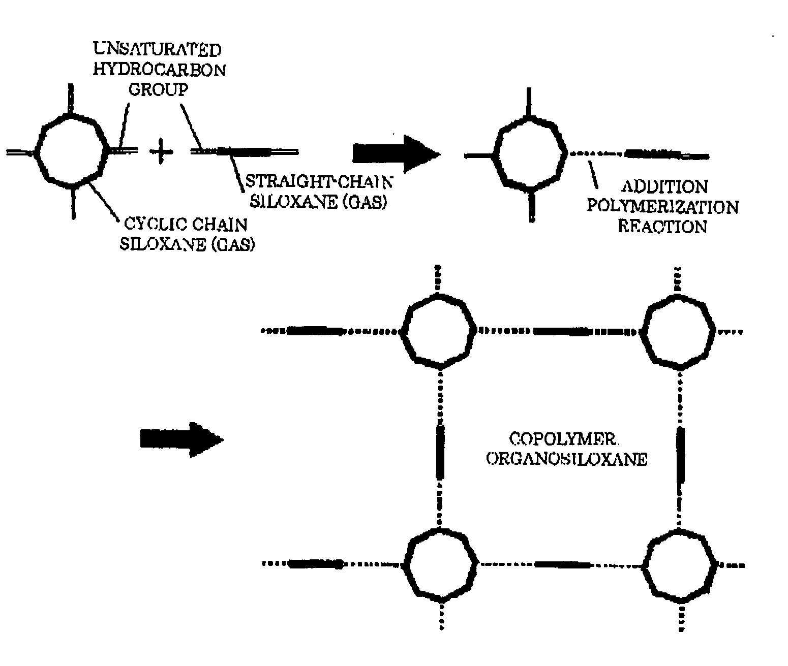
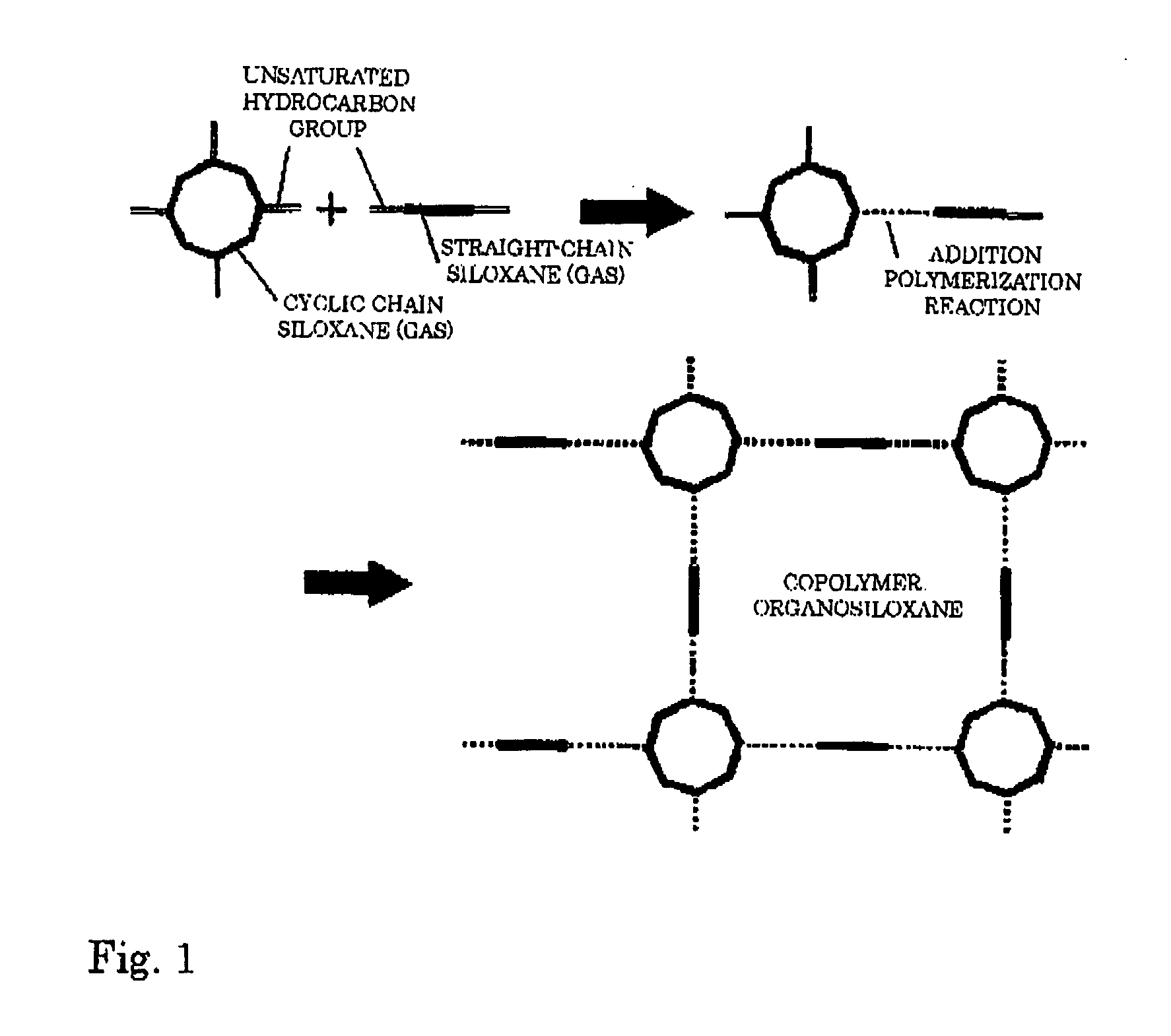
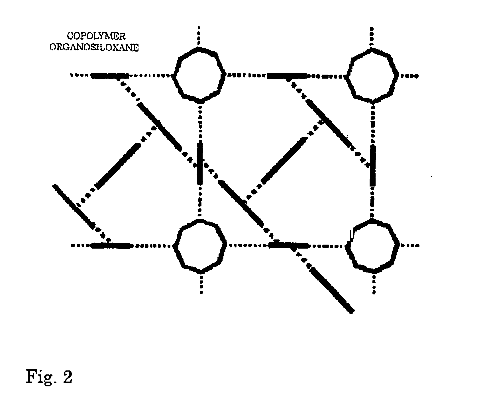
[0061] The organosiloxane copolymer film according to the present invention comprises a 4-membered cyclosiloxane composed of 4 silicon atoms and 4 oxygen atoms shown in general formula (6) below, as one of the raw materials, and as one embodiment of the first organosiloxane monomer with cyclosiloxane backbone.

General Formula (6): 4-Membered Cyclosiloxane Having a Plurality of Unsaturated Hydrocarbon Groups.

[0062] In this formula, R11V, R12V, R13V, R1a, R21V, R22V, R23V, R2a, R31V, R32V, R33V, R3a, R41V, R42V, R43V, and R4a denote hydrocarbon groups, phenyl groups or hydrogen. Specifically, tetramethylvinyl-tetramethyl-cyclotetrasiloxane (TMVTMCTS) of chemical formula (7), tetravinyl-tetramethyl-cyclotetrasiloxane (TVTMCTS) of chemical formula (8), tetramethylvinyl-tetrahydro-cyclotetrasiloxane (TMVTHCTS) of chemical formula (9), and tetravinyl-tetrahydro-cyclotetrasiloxane (TVTHCTS) of chemical formula (10) are included in one of the examples of the first organosiloxane with cyc...

second embodiment

[0067] The organosiloxane copolymer film according to the present invention uses the first organosiloxane monomer with cyclosiloxane backbone and the second organosiloxane monomer with straight-chain siloxane backbone as raw materials. One embodiment of the second organosiloxane with straight-chain siloxane backbone, is a straight-chain divinyl siloxane having a molecular structure where the terminal silicon atom of the straight-chain siloxane shown in general formula (12) below is bonded directly to vinyl group (CH2═CH—) or bonded to C═C site of the unsaturated hydrocarbon group.

General Formula (12): Divinyl Straight-Chain Siloxane

[0068] In the formula, R′1a, R′1b, R′11V, R′12V, R′13V, R′2a, R′2b, R′21V, R′22V, and R′23V denote hydrocarbon groups, phenyl groups, aliphatic hydrocarbon groups, or hydrogen. Moreover, n denotes an integer of 1 or more. Now, as examples of straight-chain divinyl siloxane having a repeating unit n=1 shown in general formula (12), are tetramethyldivin...


PUM

PropertyMeasurementUnit
dielectric constantaaaaaaaaaa

Abstract

An insulated organic copolymer is provided, having the excellent mechanical strength and deposition property at an interface contacting the lower base or the upper layer of the inorganic insulation film, and the effective dielectric constant is low as the whole film, which is suitable as the interlayer insulation film that separates the multi-layer copper wirings of the semiconductor device. The organosiloxane copolymer film is obtained by the polymerization of the cyclosiloxane and the straight-chain siloxane as the raw materials by the plasma excitation of both. At the interfaces contacting the inorganic insulation films, the interface layers having a film quality that is intricate and excellent in deposition property are prepared whereby the main component of the film composition is the straight-chain siloxane. The inner section of the copolymer film mixes the cyclosiloxane component having pores surrounded by the cyclosiloxane backbone and the straight-chain siloxane components, has the network structure layer relatively suppressing the density, and has the composition changing in the thickness direction whereby the multi-layer wirings embedding the copper thin film is formed.

Description

FIELD OF THE INVENTION [0001] The present invention relates to an organosiloxane copolymer film used as an organic insulation film for insulating between wirings that connect between elements within a semiconductor device, its production method, its deposition apparatus, and a semiconductor device using the copolymer film. More specifically, the present invention relates to a vapor-deposited organosiloxane copolymer film and a vapor deposition method of the copolymer film conforming to the application to the semiconductor devices. BACKGROUND OF THE INVENTION [0002] The design rule of a semiconductor integrated circuit is continuously being shrinked, accompanied by the performance deterioration due to wiring delay which is becoming prominent. That is, a wiring signal delay of a semiconductor integrated circuit is determined by a wiring CR time constant (C: wiring capacity, R: wiring resistance). Because of the increase in wiring resistance due to the decrease in a wire width and the ...

Claims


Application Information

Patent Timeline
Patent Type & Authority Applications(United States)
IPC IPC(8): C08G77/06C23C14/12C09D4/00C23C16/40H01L21/31H01L21/312H01L21/768
CPCC08G77/06C09D4/00C23C16/401H01L21/02126H01L21/02216H01L21/02274H01L21/3124H01L21/76835H01L21/76801H01L21/76829H01L21/76832C08G77/04Y10T428/31663
Inventor HAYASHI, YOSHIHIRO
Owner GK BRIDGE 1
Why Eureka
Try Eureka