Method for producing electronic device

a technology of electronic devices and manufacturing methods, applied in the field of lithography, can solve the problems of inability to obtain desired transistor performance, surplus leakage current generation, edge roughness present in miniaturization, etc., and achieve the effects of low cost, high integration, and high performan

Active Publication Date: 2006-05-18
RENESAS ELECTRONICS CORP
View PDF1 Cites 23 Cited by
  • Summary
  • Abstract
  • Description
  • Claims
  • Application Information

AI Technical Summary

Benefits of technology

[0011] It is a first object of the present invention to provide a method of manufacturing a semiconductor device or a semiconductor integrated circuit of high performance and high integration at low cost, using a pattern forming method of high resolution and high sensitivity and which is small in edge roughness.
[0012] It is a second object of the present invention to provide a method of processing, with high accuracy, a gate or an interconnect or hole of the semiconductor device or the semiconductor integrated circuit, while suppressing the influence of the mask defect, increase of flare light, deterioration of resolution and the like where the electron beam projection exposure method or the extreme ultraviolet (EUV) projection exposure method.
[0013] It is a third object of the present invention to provide a method of manufacturing a semiconductor device in which the thermal and mechanical characteristics of the formed pattern are improved.

Problems solved by technology

The above-described chemically amplified resist poses a problem in that edge roughness is present with miniaturization.
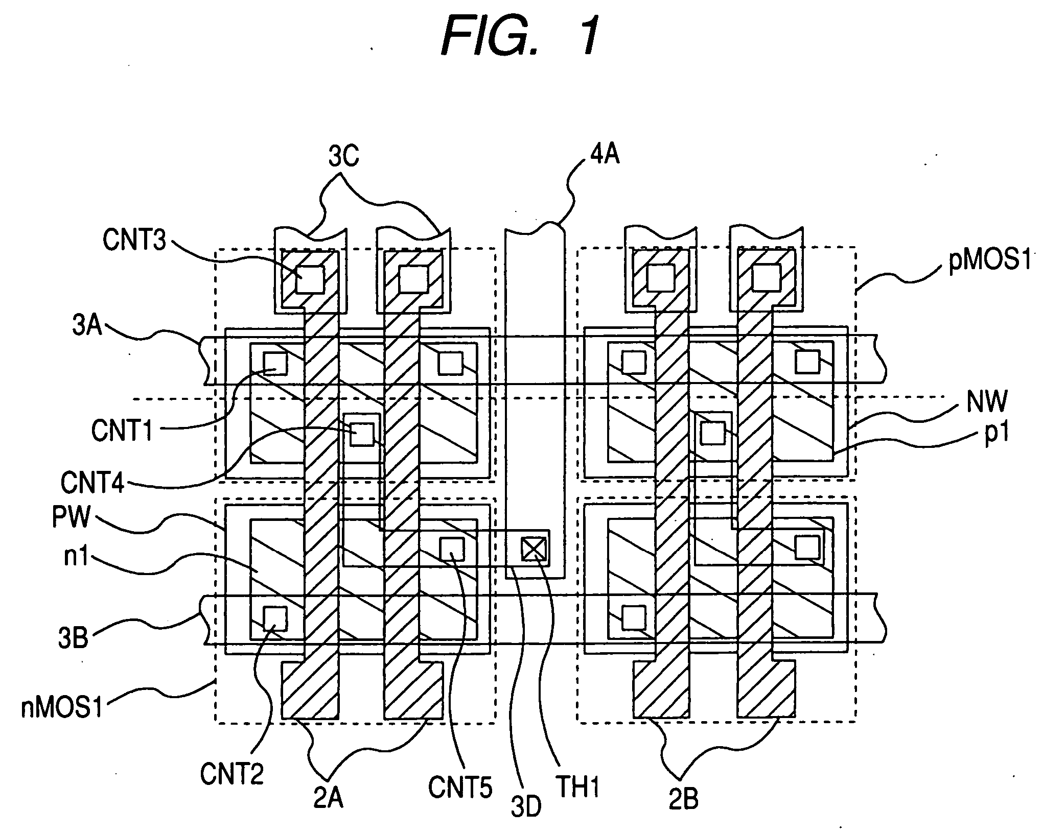
There occurs a problem in that a surplus leakage current is generated in a portion where Lg is small as shown in FIG. 11 depending on the LER and Vth features.
This results in a problem in that the desired transistor performance cannot be obtained, and the higher performance of a semiconductor device is hard to accomplish.
On the other hand, various resist materials for forming the above-described miniaturized patterns poses a problem in that even where a molecule such as calixarane is used, suppression of high resolution or roughness is hard to coexist with practical sensitivity.
For example, in the aforementioned calixarane, the roughness is small but the sensitivity is low because of non-chemically amplified resist.
However, in the cross linking negative resist, suppression of roughness is difficult due to the molecular weight by cross linking and an increase in dispersion thereof as will be mentioned later, whereas in the positive resist having a polarity conversion group introduced therein, control of solubility is difficult due to the mutual action of molecules.
Further, in the resist using fullerene, there poses a problem in that low sensitivity and development with organic solvent are necessary.
Furthermore, mechanical strength is weak, and patterns are bended due to the surface tension at the time of drying after development and rinsing.
Further, there poses a problem in that because the thermal resistance is low, the shape of resist patterns becomes broken due to the heating at the time of base etching, failing to serve as a mask at the time of base etching.
However, generally, a gate layer is low in pattern density, and therefore when the positive resist which is the main current of the conventional resist is used, it is necessary to direct an energy beam to a major region other than the gate and the interconnect pattern formed from the same layer as the gate.
However, in the F2 exposure method and EUV exposure method, there is a problem in that when the rate of light transmission portion and reflection portion on the mask is large, the probability of frequency of a mask defect increases to lower the yield.
Further, there is a problem in that when the rate of light transmission portion and reflection portion on the mask is large, flare light increases.
Further, in EPL using a stencil mask, there is a problem that when the electron beam transmission portion on the mask increases, mechanical strength becomes weak.
Further, there is a problem in that when the rate of the electron beam transmission portion is large, a mask transmission current increases so that the desired resolution (or throughput) may not be obtained due to the Coulomb effect.
However, there is a problem in that since the above-described conventional negative type resists are of the cross linking type, the roughness cannot be suppressed sufficiently.
Further, where a Cu multi-layer interconnect system using a low dielectric constant inter-layer dielectric film is formed using the so-called perforation type dual damascene method, if the conventional positive resist is used when a trench patter is formed after formation of a connection hole, a resolution defect caused by the so-called poisoning occurs.
This problem is also solved by using the negative resist, but there is a problem in that the roughness cannot be suppressed sufficiently by the conventional negative resist similar to the above.

Method used


Image

  • Method for producing electronic device
  • Method for producing electronic device
  • Method for producing electronic device

Examples


embodiment 1

[0059] As another embodiment of the present invention, an example will be described in which t-butoxycarbonylethyl-β-cyclodextrine (1) is synthesized.

[0060] Under a nitrogen current, sodium hydrate 1.7 g (0.07 mol) was diffused into tetrahydrofuran 30 ml, and a tetrahydrofuran solution 70 ml of β-cyclodextrine 11.3 g (0.010 mol) was dropped. After dropping, it was stirred at room temperature for about 30 minutes, after which bromoacetic acid t-butyle ester 13.7 g (0.07 mol), and tetra-n-butyl ammonium bromide 1.1 g (3.5 mol) were added at once, and refluxing was carried out for 3 hours. Then, a reaction solution obtained was poured into water 40 ml, extraction was done with ethyl acetate, and an organic layer was washed with water three times. The organic layer was dried with sodium sulfate, after which sodium sulfate is filtered, a solvent was removed under reduced pressure from the filtrate for concentration, precipitated again with n-hexane, and then dried to thereby obtain t-bu...

embodiment 2

[0079] As another embodiment of the present invention, an example in which 1-ethoxy ethyl calyx [4] resorcinol arene (IV) was synthesized will be described hereinafter. Resorcinol 10.0 g, aceto aldehyde 4.0 g, and distilled water 60 g were stirred, and undiluted sulfuric acid 10 ml was slowly dropped thereon. After dropping, it was refluxed for 4 hours at 70° C., water of 1 l was added after termination of reaction and stirred for about 10 hours. Thereafter, a solid portion was filtered and re-crystallized with ethanol to obtain calix [4] resorcinol arene 11.5 g.

[0080] Next, calix [4] resorcinol arene 10.9 g (0.020 mol) is dissolved into tetrahydrofuran 100 ml, into which were put ethyl vinyl ether 13.8 g (0.192 mol) and pyridinum-p-toluene sulfonate 0.90 g and closely plugged, and reacted for 10 hours. After reaction, ethyl acetate 200 ml was added, and washed with 150 ml water three times. Thereafter, it was dried with sodium sulfate, sodium sulfate was filtered, filtrate was con...

embodiment 3

[0097] As another embodiment of the present invention, an example will be described in which t-Butoxy carbonyl methyl fullerene is synthesized.

[0098] Under a nitrogen current, sodium hydrate 0.17 g (7.0 mol) was diffused into tetrahydrofuran 10 ml, and commercially available aqueous fullerene C60(OH)n(n=22-26) 1.13 g (1.0 mmol) was additionally diffused to a tetrahydrofuran solution 10 ml. It was stirred at room temperature for about one hour, after which bromoacetic acid t-butyle ester 0.14 g (7.0 mmol), and tetra-n-butyl ammonium bromide 0.011 g (0.035 mmol) were added at once, and heating was carried out for one hour at 60° C. Then, the reaction solution obtained was poured into water 40 ml, and the separation was filtered and washed with water to obtain t-Butoxy carbonyl methyl fullerene 1.05 g (molecular weight 1933).

[0099] The thus obtained t-Butoxy carbonyl methyl fullerene 100 parts by weight, acid generator triphenyl sulfonium nonafrate 5 parts by weight, and phenyl pyriz...


PUM


Abstract

There is a problem in that when the demand accuracy with respect to a semiconductor pattern dimension comes close to a resist molecule size with miniaturization, the device performance is deteriorated due to edge roughness of a resist pattern to exert a bad influence on the system performance. The present invention overcomes the problem by the procedure in which super-molecules which are small in dimension as compared with the conventional polymers are used as main components, the reaction number required for the change of molecule solubility is made constant and as large as possible, and an acid generator is made clathrate or combinatory n super molecules to make an acid catalyst concentration large. As a result, it is possible to form a pattern of molecular accuracy with high productivity even with respect to the pattern dimension less than 50 nm, thereby realizing the high performance system.

Description

TECHNICAL FIELD [0001] The present invention relates to a method of manufacturing electronic devices such as semiconductor integrated circuits, and particularly relates to lithography processes for forming the circuit patterns with high accuracy, and a radiosensitive chemical compound used therefor. BACKGROUND ART [0002] At present, in the semiconductor integrated circuits, miniaturization of circuit pattern feature is progressing, and particularly shortening of a gate length of CMOS transistors and reduction of an interconnect pitch are being accelerated. With this, critical dimension accuracy is required for these circuits. The leading resist material used to form presently latest miniature circuit patterns is the so-called chemically amplified resist. The photo acid generation agents which generate acid by exposure are dispersed into the matrix resins, and solubility of the matrix resins is changed by catalytic reaction of acid generated in the exposure section. For example, in t...

Claims


Application Information

Patent Timeline
Patent Type & Authority Applications(United States)
IPC IPC(8): G03C5/00G03F7/004G03F7/038G03F7/039G03F7/075
CPCG03F7/0045G03F7/0382G03F7/0392G03F7/0755G03F7/0757H01L21/31144H01L21/32139H01L21/76808H01L27/10
Inventor FUKUDA, HIROSHIYOKOYAMA, YOSHIYUKIHATTORI, TAKASHISAKAMIZU, TOSHIOARAI, TADASHISHIRAISHI, HIROSHI
Owner RENESAS ELECTRONICS CORP
Why Eureka
Try Eureka