Bandgap-shifted semiconductor surface and method for making same, and apparatus for using same

Inactive Publication Date: 2008-11-20
NANOPTEK CORP
View PDF22 Cites 28 Cited by
  • Summary
  • Abstract
  • Description
  • Claims
  • Application Information

AI Technical Summary

Benefits of technology

[0031]One would like a semiconductor photocatalyst with a bandgap that is better matched to the solar spectrum and/or artificial illumination for higher efficiency or even to work at all. In this invention, the bandgap of the known chemically-inert photocatalyst titania (TiO2) is shifted and broadened to be active at wavelengths more prevalent in sunlight and artificial light by inducing and managing sufficiently high stress in titania by vacuum coating a thin film of titania onto a substrate, preferably of a different Young's modulus, with bending undulations on the surface of a spatial radius similar to the film thickness. The undulated coating also serves to self-focus and concentrate the

Problems solved by technology

The ills of our carbon-based energy are well-known: pollution of land and oceans, air pollution, and the global warming that is likely caused by the latter.
In addition, there is the growing dependence on foreign oil (presently at 46%, up from 27% during the Oil Embargo during the Carter administration) with the economic, political, and human costs that result from that dependence.
However, the losses of the solar cell in converting sunlight to electricity, combined with the losses in the electrolytic splitting of water into hydrogen and oxygen, make for low efficiency overall.
Further, the cost of the apparatus and lifetime of the components make the economic viability dim at this time.
However, the threshold energy for this reaction is 6.5 eV, so direct photodissociation is not possible.
Even so,

Method used


Image

  • Bandgap-shifted semiconductor surface and method for making same, and apparatus for using same
  • Bandgap-shifted semiconductor surface and method for making same, and apparatus for using same
  • Bandgap-shifted semiconductor surface and method for making same, and apparatus for using same

Examples


example 1

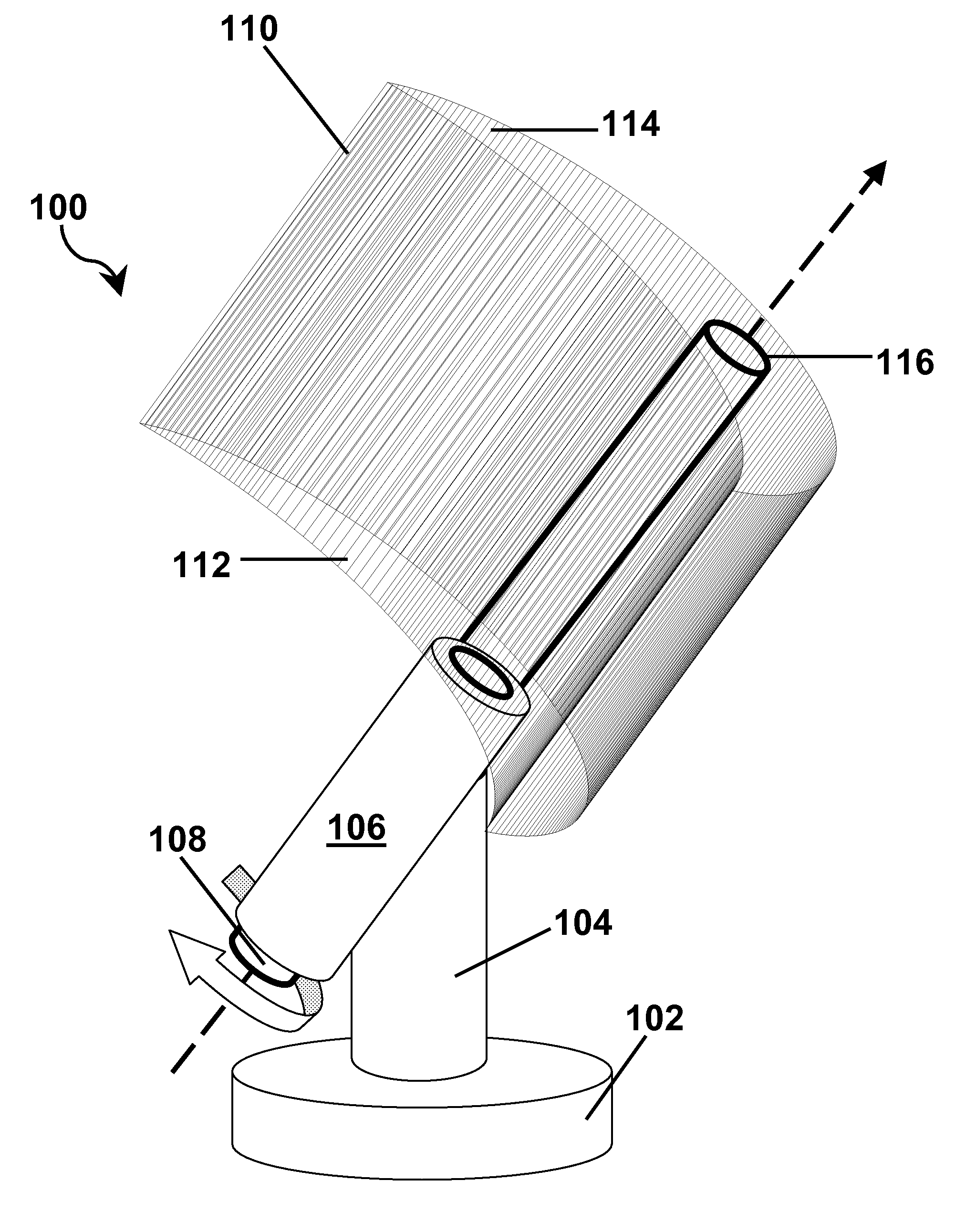
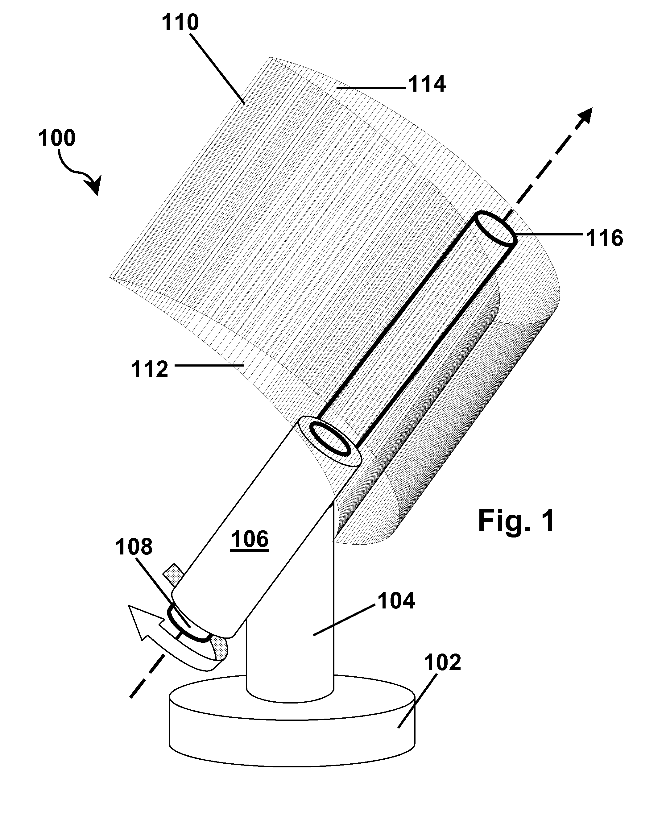
[0146]This Example illustrates the effects of illumination conditions, bias voltage and temperature on the efficiency of hydrogen production and conversion efficiency of an apparatus as shown in FIGS. 1-2 and 7.

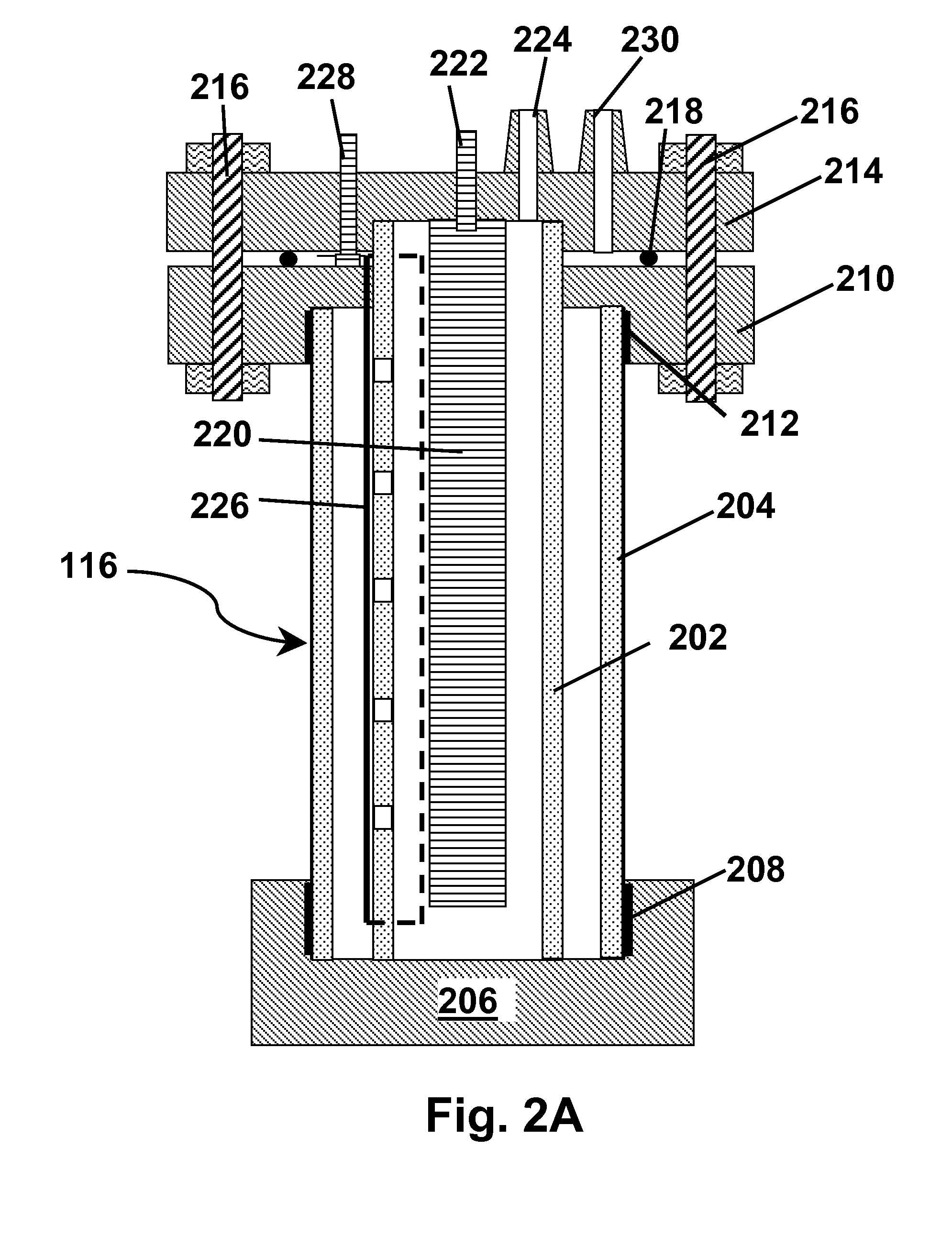
[0147]An apparatus as described above with reference to FIGS. 1-2 and 7 was subjected to artificial solar illumination conditions of AM 1.5 and AM 0.0, where AM means Air or Atmospheric Mass, the amount of atmosphere through which the sunlight must travel to reach the ground. So, AM 1.5 is typical for sea level conditions, while AM 0.0 is for a “space” application such as orbiting satellites. with the core assembly 116 maintained at either 25 or 80° C. and with varying bias voltages applied between the photoactive anode 226 and the cathode 220. In these tests, the bias voltage was not supplied by the photovoltaic strip 602 (FIG. 7) in order to permit the illumination of the photovoltaic strip and the bias voltage to be controlled independently. FIG. 13A shows the rate of hydr...

example 2

[0149]This Example illustrates (see FIG. 14) the effects of bias voltage on conversion efficiency of an apparatus as shown in FIGS. 1, 2 and 7, as a function of the electrolyte composition. The best results, i.e. highest hydrogen production efficiency, are obtained with either an acidic electrolyte or a salt water electrolyte. The basic potassium hydroxide electrolyte performs best at zero voltage bias, but underperforms at higher voltage bias.

[0150]The photoactive titania electrodes of the present invention can be used in any application in which photoactive titania electrodes have hitherto been used, as discussed in detail in the aforementioned parent application.

[0151]In summary, this invention provides for shifting the optical bandgap of a semiconductor into longer optical wavelengths by stressing the semiconductor, where the semiconductor is a thin film, and where the stress is strain caused by some or all of the following: conditions under which the thin film is formed, the sh...


PUM

PropertyMeasurementUnit
Electric potential / voltageaaaaaaaaaa
Wavelengthaaaaaaaaaa
Conductionaaaaaaaaaa

Abstract

Apparatus for generating electricity and for carrying out photo-induced reactions comprises: a primary reflector (610) or other optic which concentrates radiation to a primary focus; a secondary reflector at the primary focus to direct radiation to a secondary focus; a photovoltaic device (602) to convert radiation to electricity; and a photo-reactor (116) having a photoactive electrode, one of the photovoltaic device (602) and the photoactive electrode (116) lies at the primary focus, and the other at the secondary focus. Electric potential generated by the photovoltaic device (602) may be used to provide a bias or over-voltage between the photoactive electrode and a counter electrode. The apparatus may be used to photolyze water or to carry out other photochemical reactions.

Description

REFERENCE TO RELATED APPLICATIONS[0001]This application is a continuation-in-part of copending application Ser. No. 10 / 424,259, filed Apr. 26, 2003 (Publication No. 2003 / 0228727), which claims benefit of Provisional Application Ser. No. 60 / 380,169, filed May 7, 2002. This application is also related to copending application Ser. No. 12 / 136,716, filed Jun. 10, 2008. The entire disclosures of all three of these applications are herein incorporated by reference.BACKGROUND OF INVENTION[0002]This invention relates to a bandgap-shifted semiconductor surface, and a method for making same. This invention also relates to photocatalytic surfaces used in the process of photoelectrolysis, photovoltaics, and photocatalysis, and more specifically to induction and management of stress in a thin titania film photocatalytic surface to match the band gap of the titania more efficiently with the solar spectrum at the earth's surface for photoelectrolysis, photovoltaics, and photocatalysis.[0003]For ge...

Claims


Application Information

Patent Timeline
IPC IPC(8): B01J19/08H01L31/0232H01L31/04
CPCB01J21/063B01J35/004B01J37/0226C01B3/042C01G23/047H01L31/0547Y02E10/52Y02E60/364H01M14/005H01L31/0543C25B1/003C25B1/55Y02E60/36
Inventor GUERRA, JOHN M.
Owner NANOPTEK CORP
Why Eureka
Try Eureka