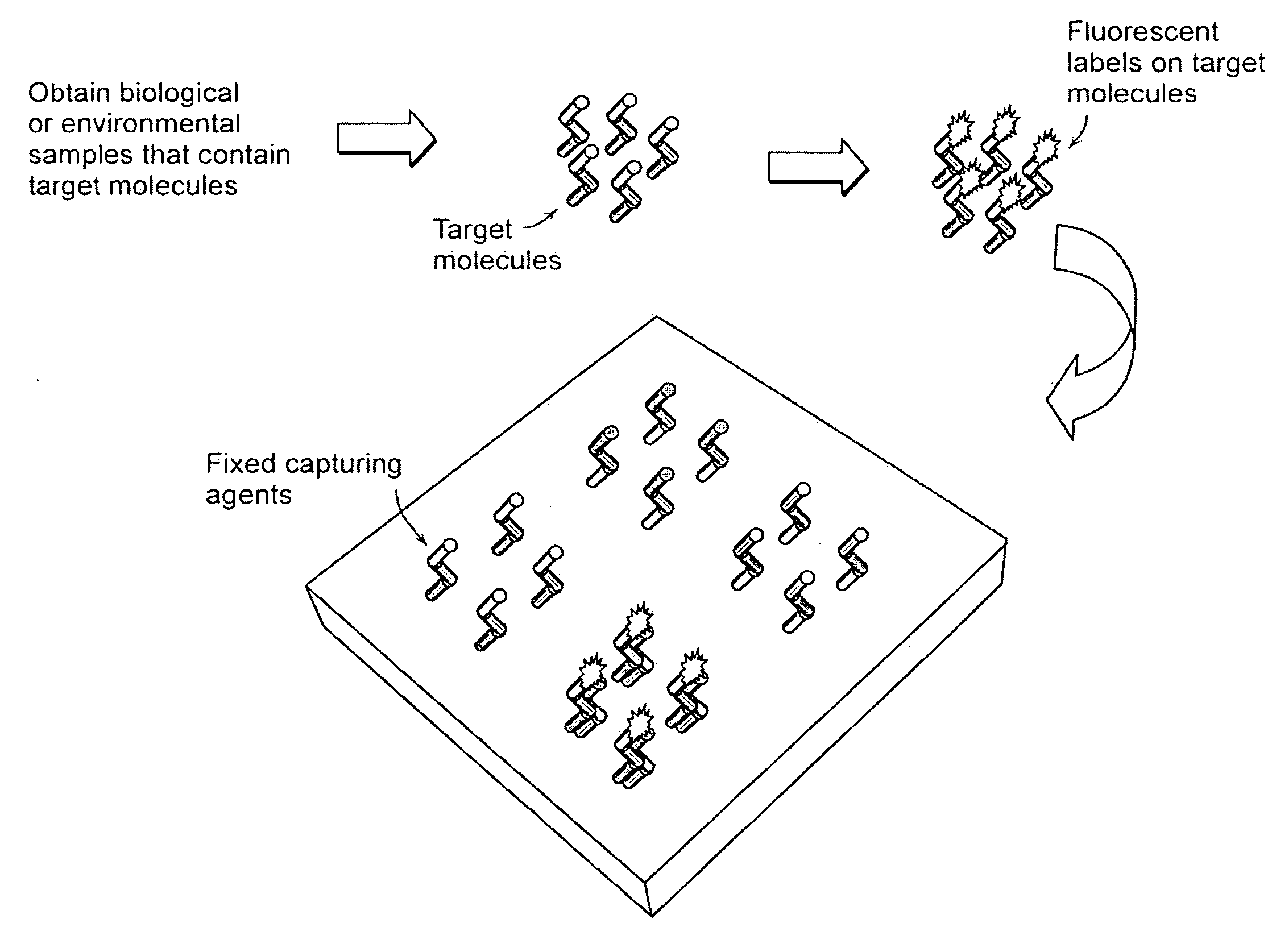
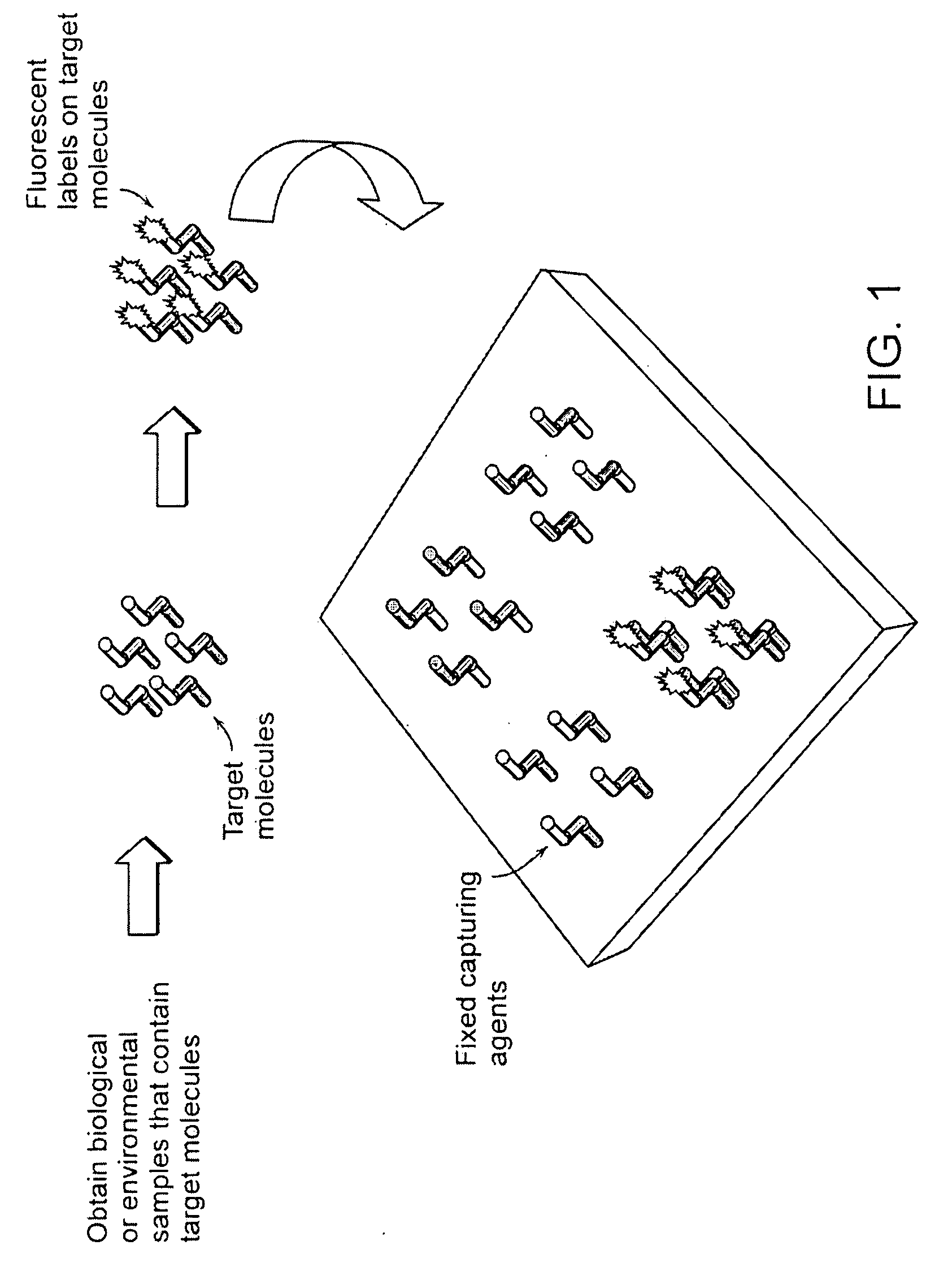
[0080]
Microarray technology, including methods for making microarrays, procedures for conducting
microarray experiments, and applications are well known in the art [see, for example, Schena 2000]. The
chemistry for the attachment of capture molecules to SiO2 substrates (i.e., the
coating layer) are also well known in the art. A significant
advantage of the present invention over current microarray detection methodologies is that the present techniques eliminate the need to detectably label the target molecules prior to performing the binding reaction on the microarray. A second
advantage of the present techniques described herein is that a baseline height scan of the microarray may be performed prior to running the binding reaction with the target molecules so that the height of each detection location may be compared before and after target molecule binding. This eliminates the need for height and / or density uniformity of the capture molecules across the entire microarray. It also serves to reduce interexperimental variability (e.g., that result from manufacturing defects) where replicate microarrays are compared.
[0081]An exemplary microarray useful in accordance with the principles of this disclosure may be created on the layered substrate by first cleaning the
substrate surface with
acetone,
methanol, water, and N2 gas, then
etching the surface with 10% NaOH for about 10 minutes. The surface is next silanized and functionalized with an amino-
silane (for instance: 3-aminopropyl-
triethoxysilane). Capture DNA is then be spotted at spatially distinct locations on the surface using a hollow pin (usually done robotically), using standard ink-jet printing technology [Hughes 2001], or using standard
photolithography techniques [Singh-Gasson 1999]. The DNA is cross-linked (covalently bonded) to the surface by
irradiation with UV light. The surface is finally rinsed before use.
Alternative methods exist for making arrays including methods that use
photolithography.
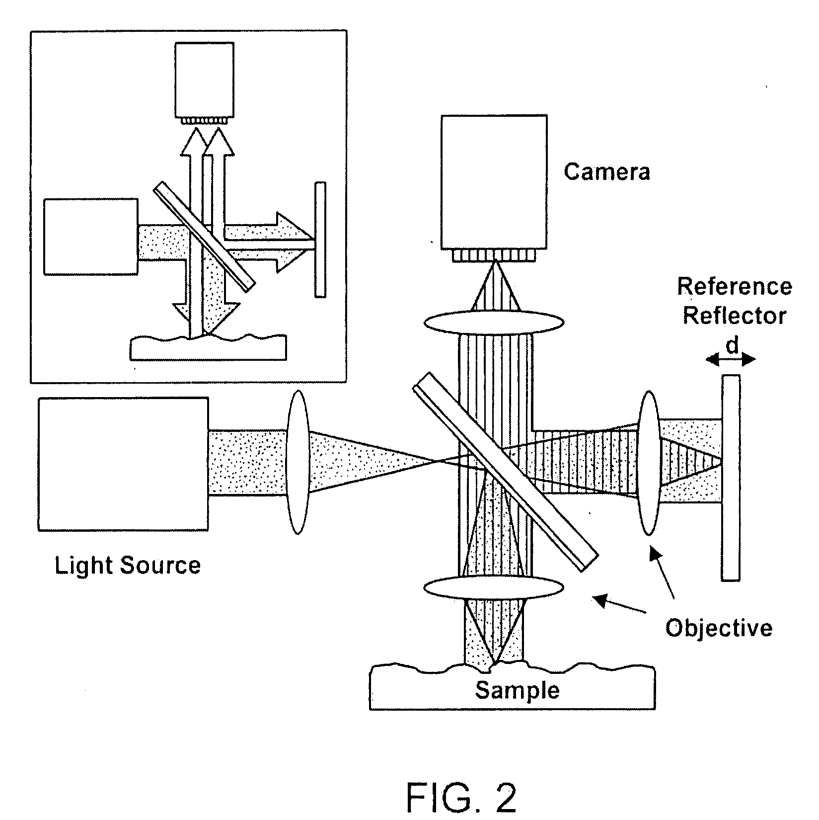
[0082]The microarray is then scanned using any method in accordance with the principles of this invention to determine the initial height of each location. Next, target DNA is introduced to the surface via a solution, rinsed, and dried. The array is scanned again using the same method and the increase in height is recorded for each location. The change in height is an index of the amount of target DNA bound to that location.E. Alternative Substrate Designs
[0083]SiO2 layered on Si, as described above, is the simple case of a layered substrate that can be used in accordance with the principles of this disclosure. More complex layered substrates may also be used. The most desirable property for layered substrates is that the beam reflected from the target molecule surface undergoes a
maximum phase change for a small change in the amount of material bound. A layered substrate consisting of many semitransparent
layers of different optical indices can exhibit a very rapid change in both the intensity and phase of the reflected light for a small amount change in
wavelength. Similarly, such a structure may exhibit a very rapid change in phase for a small amount of material modifying the thickness of the top layer. For example, a stack consisting of 270 nm of SiO2, 340 nm of Si, 270 nm of SiO2, 340 nm of Si, and 270 nm of SiO2 on an
Si substrate has
high reflectivity for wavelengths of 1550 nm. If the top SiO2 layer is slightly modified with binding molecules, the
reflectivity will remain high, but the phase will change rapidly. This rapid
phase change will give an enhanced
signal in either of the split beam
interferometry methods described above.
[0084]The key is to create layered substrates that cause a rapid change in the phase of the reflecting light resulting from a small change in surface height. Materials may be used other than Si and SiO2. Alternative
coating layers that are useful in layered substrates include
dielectric substances such as Si3N4.
[0085]In addition to the standard substrate configurations such as
surface coating with capture molecules, either as a film or in spatially discrete locations as a microarray, alternative configurations may be useful depending upon the application. For example, in one alternative embodiment, an additional discontinuous layer is formed on top of the
coating layer such that individual reaction wells are created. These reaction wells are desirably about 200 μm×200 μm×1 mm, but any convenient size may be used, depending upon the specific application and
reaction conditions. These reaction wells may serve to contain the bonding reaction that fixes the capture molecules to the
substrate surface, or the wells may be used to contain individual binding reactions in spatially and / or chemically distinct environments. FIG. 12 illustrates a layered substrate 500 having a base layer 121, a top coating layer 122a and an intermediate coating layer 122b built in accordance with the principles of this disclosure. The layered substrate 500 further comprises reactions wells 575 formed by well walls 570. Each reaction well 575 may contain the same or different reactants (e.g., target molecules, capture molecules, biological / environmental samples), in a
liquid medium, as the other reaction wells 575 on the same layered substrate 500. The reaction wells 575 may be formed by layering a polymeric (e.g., PDMS) or other coating material (e.g., SiO2) on top of the top coating layer 122a. Alternatively, the reaction wells 575 may be formed by
etching or
soft lithography such that the wells are “
cut” into the top coating layer 122a. For convenience, the layered substrate 500 is shown in conjunction with the direct
reflectivity measurement apparatus, but these substrates are also useful with either the split beam
interferometry or the modified split beam inferometry methodologies of this disclosure.F. Real-Time
Instrument Design

