

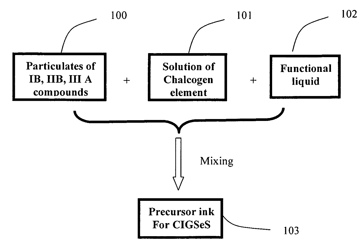
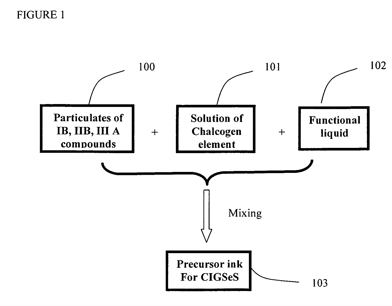
Precursor ink for producing IB-IIIA-VIA semiconductors
a technology of semiconductors and precursor inks, applied in the field of precursor inks, can solve the problems of low pv performance, low efficiencies, and difficulty in deposited uniform films with exact atomic ratios on large areas using vapor phase processes
- Summary
- Abstract
- Description
- Claims
- Application Information
AI Technical Summary
Benefits of technology
Problems solved by technology
Method used
Image

Examples
embodiment 1
[0024]A mixture of 0.334 g of copper acetate, 0.413 g of indium acetate, and 0.223 g of gallium acetone acetate is ball-milled in the liquid of isopropanol (8 mL) into fine particle (with size less than 0.8 micrometer) and then mixed in a solution of selenium (0.319 g dissolved in 5 ml of trioctyl phosphine) in trioctyl phophine to form the precursor Ink 1.
[0025]A molybdenum-coated soda-lime glass substrate is dipped in Ink 1 at room temperature, and the coated substrate is dried in a vacuum at 220° C. for 2 hours. The dried substrate is then sealed in an autoclave and heated to 500° C. in argon. This reaction forms a copper-indium-gallium diselenide (CIGS) film with a thickness of about 2 μm and a composition of CuIn0.77Ga0.33Se2.1. This film can form a light absorbing semiconducting layer for a thin film photovoltaic cell.
embodiment 2
[0026]A mixture of 3.18 g of copper oxide nanoparticles (diameter less than 0.2 micrometer) and 5.55 g of indium oxide nanoparticles diameter less than 0.2 micrometer) is suspended in a solution of 44 g of pentacanoic acid in 20 mL of butyl acetate. This suspension is mixed into a solution of 6.32 g of selenium in 40 ml of trioctyl phosphine to form the precursor Ink 2.
[0027]A molybdenum coated soda-lime glass substrate is coated with Ink 2 while spinning, and the coated substrate is vacuum dried at 220° C. for 2 hours. The dried substrate is sealed in an autoclave chamber and heated to 500° C. in argon. The copper, indium and gallium in the film react to form a 2 μm film of CuInSe2. This film can form a light absorbing semiconducting layer for a thin film photovoltaic cell.
embodiment 3
[0028]A solution of selenium is prepared by adding 1.74 g selenium into the solvent of trioctylphophine (10 mL) and stirred for 3 days. A mixture of 0.80 g of copper oxide nanoparticles and 1.39 g of indium oxide nanoparticles is suspended in the selenium solution in trioctylphophine. A dilution solution of ethyl acetate (3 mL) is added into the solution to adjust thickness. And polyacrylic acid (with sodium) (0.134 g of 1% solution in water) was added into the mixture ink to adjust viscosity and to adjust sodium dopant. The ink was then stirred vigorously for 12 hours to form Ink 3.
[0029]A molybdenum coated soda-lime glass substrate is coated with Ink 3 by a rod coating method, and the coated substrate is vacuum dried at 220° C. for 2 hours. The dried substrate is put into a sufurization tube and heated to 480° C. for 30 minutes and followed with 510° C. for 2 hours under a stream of hydrogen sulfide (2% balanced in argon) with a flow speed of 0.5 mm / minute. The copper, indium in t...
PUM
 Abstract
Description
Claims
Application Information