
Composition comprising chelating agents containing amidoxime compounds

a technology of amidoxime and compound, which is applied in the field of composition comprising amidoxime compound, can solve the problems of ruthenium or molybdenum, difficult removal of unreacted metal, and difficult effective removal, so as to achieve the effect of providing for the chelation of metal ions residues

Inactive Publication Date: 2010-04-29
EKC TECH
View PDF28 Cites 82 Cited by
  • Summary
  • Abstract
  • Description
  • Claims
  • Application Information

AI Technical Summary

Benefits of technology

[0067]Many formulations being used in cleaning substrates containing metallic-etch residue removal, post-CMP cleaning, and other semiconductor applications, contain complexing agents, sometimes called chelating agents. Much metal-chelating functionality are known which cause a central metal ion to be attached by coordination links to two or more nonmetal atoms (ligands) in the same molecule. Heterocyclic rings are formed with the central (metal) atom as part of each ring. When the complex becomes more soluble in the solution, it functions as a cleaning process. If the complexed product is not soluble in the solution, it becomes a passivating agent by forming an insoluble film ...

Problems solved by technology

Some of the likely candidates, such as ruthenium or molybdenum, are likely to pose major challenges for wet processing, particularly in relation to the decontamination of the wafer backside.
An undesired by-product of the chemical vapor or atomic layer deposition used to deposit these materials is the deposition of films on the wafer backside.
A wet etch will likely be necessary to remove the deposited films from the backside of the wafer and to prevent front-side contamination issues and effective removal will likely be difficult.
Nickel will likely provide a challenge for selective frontside etch and backside decontamination.
The addition of even 5% platinum may introduce a challenge to remove the unreacted metal after the salicidation process.
Platinum metal is difficult to wet etch, and efforts to identify appropriate solutions are ongoing.
In BEOL cleaning, metal layers are present on the wafers and the allowable cleaning solutions are limited versus FEOL cleaning.
The integration of dual metal gates for CMOS fabrication is challenging and requires a selective removal of the first metal prior to depositing the second one, such as Ti and Ta-based metals and the underlying high-k such as SiON, HfO2, RuO2 or HfSiO(N) etc. which will require further optimization of the cleaning solutions and / or complete removal of the underlying gate dielectric to reduce the metal contamination below the detection limit.
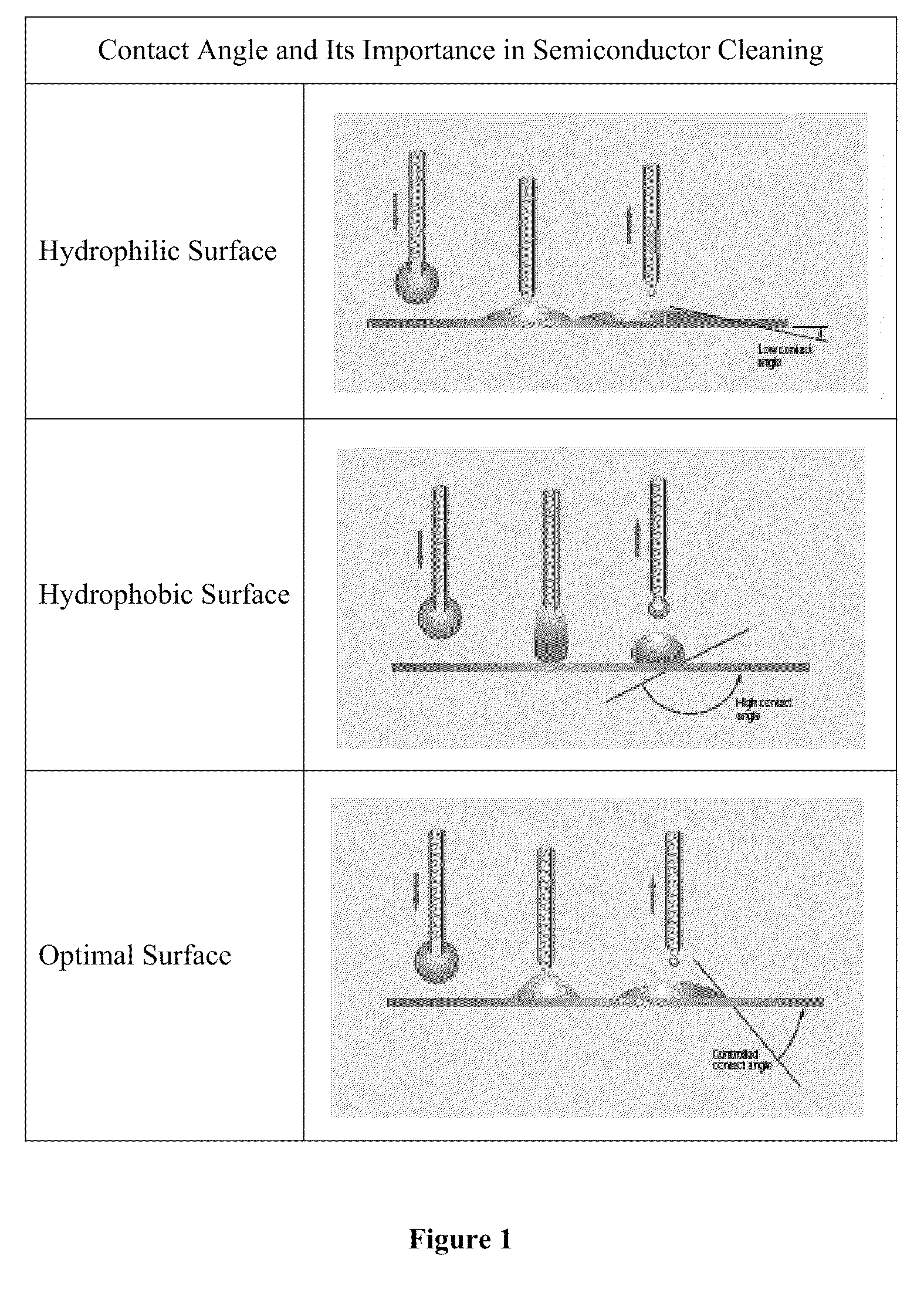
Hydrophobic surfaces are more difficult to clean because cleaning solutions do not wet as well and during drying, the solutions tend to “bead” up on the surface, leaving particles on the surface instead of maintaining the particles in solution.
Another common problem with cleaning semiconductor surfaces is the deposition of contaminants on the surface of the semiconductor device.
Any cleaning solutions that deposit even a few molecules of an undesirable composition, such as carbon, will adversely affect the performance of the semiconductor device.
Cleaning solutions that require a rinsing step can also result in depositing contaminants on the semiconductor surface.
It is no longer valid that FEOL cleaning involves only silicon or silicon oxide.
Otherwise, ineffective residue removal has the potential for high levels of process defects, and the quality of the cleaning step can directly impact electrical yield.
This process is costly and hazardous and also does not effectively remove inorganic residues such as implant species, silicon, silicon dioxide and resist additives.
Moreover, such dry ashing followed by those wet chemistry cleans causes unwanted damage to the doped wafers, i.e., to the source and drain areas of the doped wafer.
Other problems are related to the fact that some of the dielectric materials are easily attacked by wet chemicals (e.g., hafnium silicates, tantalum-based dielectrics, etc.), and there is also the possibility of galvanic corrosion of the gate electrode if different materials, such as polysilicon are in contact on top of the metal.
H2O2 also has a limited bath life and decomposes over time.
Insufficient H2O2 levels in SC1 baths can lead to surface pitting and insufficient H2O2 levels in SPM baths lead to carbon build-up in the bath and poor removal of organic contaminants.
The SC1 solution, however, leaves metallic contaminants behind.
In some cases, the biodegradability of the above mentioned chelating agents are unsatisfactory.
For example, EDTA proves to have inadequate biodegradability in conventional tests, as does PDTA or HPDTA, and corresponding aminomethylenephosphonates which, moreover, are often undesirable because of their phosphorus content, phosphorus (P) is one of the dopant for silicon.
In juxtaposition, cleaning needs and goals have become more demanding.
In some cases, the biodegradability is also unsatisfactory.
Thus, EDTA proves to have inadequate biodegradability in conventional tests, as does PDTA or HPDTA and corresponding aminomethylenephosphonates which, moreover, are often undesirable because of their phosphorus content.
This presents a problem for formulators where a chelating function is sought but only selectively to metal oxide and not the metal itself, e.g in an application involving metal, such as copper.

Method used


Image

  • Composition comprising chelating agents containing amidoxime compounds
  • Composition comprising chelating agents containing amidoxime compounds
  • Composition comprising chelating agents containing amidoxime compounds

Examples


example of embodiments

of the Present Invention

[0315]In an exemplary embodiment, the compositions comprising an amidoxime compound are further diluted with water prior to removing residue from a substrate, such as during integrated circuit fabrication. In a particular embodiment, the dilution factor is from about 10 to about 500.

example 1

[0316]The patents and publications referred to in the specification are hereby incorporated by reference in their entireties. An exemplary embodiment involves a method for removing organometallic and organosilicate residues remaining after a dry etch process from semiconductor substrates. The substrate is exposed to a conditioning solution of phosphoric acid, hydrofluoric acid, and a carboxylic acid, such as acetic acid, which removes the remaining dry etch residues while minimizing removal of material from desired substrate features. The approximate proportions of the conditioning solution are typically 80 to 95 percent by weight amidoxime compound and acetic acid, 1 to 15 percent by weight phosphoric acid, and 0.01 to 5.0 percent by weight hydrofluoric acid. See, U.S. Pat. No. 7,261,835.

[0317]Another exemplary embodiment includes from about 0.5% to about 24% by weight of complexing agents with amidoxime functional groups with an aqueous semiconductor cleaning solution having a pH ...

example 2

[0318]Table 1 lists other exemplary embodiments of the present invention where the formulations additionally include from about 0.5% to about 24% by weight of compounds with amidoxime functional groups in aqueous semiconductor cleaning solutions. Such formulations may contain additional components consistent with this application such as surfactants, alkaline components, and organic solvents.

TABLE 1Exemplary Formulations with Chelating Agents for Usewith Amidoxime CompoundsH3PO4 (wt %)Other Acidwt %2methanesulfonic1.472pyrophosphoric acid (PPA)3.02Fluorosicilic0.242Oxalic2.04Oxalic2.06Glycolic1.03Oxalic2.03Lactic2.04Lactic2.03Citric2.04Citric2.03PPA0.53Glycolic2.06Glycolic2.03PPA2.03PPA4.0


PUM


Abstract

The present invention is a novel aqueous cleaning solution for use in semiconductor front end of the line (FEOL) manufacturing process wherein the cleaning solution comprises at least one amidoxime compound.

Description

BACKGROUND[0001]Front End Of Line processes (FEOL) perform an operation on a semiconductor wafer in the course of device manufacturing up to first metallization. Back End Of Line processes (BEOL) perform an operation on a semiconductor wafer in the course of device manufacturing following first metallization.[0002]A large number of complexing agents for metal ions are used in a wide variety of applications, such as: semiconductor cleaning, detergents and cleaners, electroplating, water treatment and polymerizations, the photographic industry, the textile industry, the papermaking industry, pharmaceuticals, cosmetics, foodstuffs and plant feeding.[0003]The present invention relates to the field of semiconductor processing and more specifically to a cleaning solution and a method of using the cleaning solution for Front End Of Line processes (FEOL) in a semiconductor manufacturing cleaning process.[0004]Metal gate materials are currently being introduced in conjunction with high-k gat...

Claims


Application Information

Patent Timeline
IPC IPC(8): C11D7/18C11D7/32
CPCC09G1/02C11D3/323C11D7/3272C11D11/0047G03F7/425H01L21/3212H01L21/02052H01L21/02057H01L21/02063H01L21/02074H01L21/31111H01L21/02024C11D2111/22
Inventor LEE, WAI MUN
Owner EKC TECH
Features
  • Generate Ideas
  • Intellectual Property
  • Life Sciences
  • Materials
  • Tech Scout
  • Unparalleled Data Quality
  • Higher Quality Content
  • 60% Fewer Hallucinations
Learn More