Sputtering target, transparent conductive film and transparent electrode

a technology of conductive film and electrode, applied in the direction of conductive materials, conductive materials, cable/conductor manufacturing, etc., can solve the problems of reducing the content of indium in ito, retarding the film forming speed, and difficult to reduce the content of indium to 90 atomic percent or less, etc., to achieve the effect of reducing the content of indium, etching properties, and improving the conductivity

Active Publication Date: 2010-07-08
IDEMITSU KOSAN CO LTD
View PDF17 Cites 61 Cited by
  • Summary
  • Abstract
  • Description
  • Claims
  • Application Information

AI Technical Summary

Benefits of technology

[0021]The inventors of the invention have found that among many combinations of the compounds, a combination of a spinel structure compound of Zn2SnO4 and a bixbyite structure compound of In2O3 has a low resistance and a high theoretical relative density, and can form a target with a high strength. Although the reason for this effect cannot completely be elucidated, it is assumed that under specific sintering conditions in specific compositions, In is easily dissolved as a solid solute in a spinel structure compound of Zn2SnO4, and Sn and the like are easily dissolved as a solid solute in a bixbyite structure compound of In2O3. That is, it is assumed that when positive divalent Zn exists, positive tetravalent Sn is easily dissolved in In2O3 containing positive trivalent In as a solid solute, whereas when positive divalent Zn and positive tetravalent Sn are present in proximate, positive trivalent In is easily dissolved in Zn2SnO4 as a solid solute.
[0022]Moreover, the inventors of the invention have found that if the crystal structure of a target is substantially a bixbyite structure, the target can exhibit the same etching workability as IZO and the same film performance as the ITO, even if the indium content is reduced to 60 to 75 atomic percent.
[0023]The inventors of the invention have further found that the transparent conductive film formed by the sputtering method using these targets excels in conductivity, etching properties, heat resistance, and the like, and is suitable for various applications such as a display represented by a liquid crystal display, a touch panel, a solar cell, and the like even if the content of indium is reduced.

Problems solved by technology

Although ITO has excellent properties as a material for transparent conductive oxide, ITO is not only a scarce resource, but also contains a large amount (about 90 atomic percent) of indium which is a biologically harmful element.
If an abnormal electrical discharge occurs, scattered materials become attached to the transparent conductive oxide as impurities during or immediately after the film formation.
The indium content in ITO must be reduced due to these problems of instability of supply (scarcity) and hazardous properties.
Therefore, it is difficult to reduce the content of indium to 90 atomic percent or less.
However, if the indium content is reduced to 90 to 70 atomic percent or less in this method, there are problems such as decrease of the sintered density and conductivity of the target, which causes abnormal electrical discharge and retards the film forming speed; low target strength, leading to easy cracking; and poor heat resistance in the presence of air of the transparent conductive film formed by sputtering.
This brings about another problem of a high industrial manufacturing cost.
Furthermore, the hexagonal layered compound has no resistance to an etching solution containing phosphoric acid used for etching of a metal or an alloy.
Thus etching of the metal or alloy membrane formed on the film of the hexagonal layered compound is difficult.
However, this method has problems such as difficulty in sputtering due to unduly high target resistance and a tendency of easy generation of abnormal electrical discharge.
No study of a sputtering target to solve these problems has been undertaken.
However, no studies have been done on the effect of a sintered body having both a spinel structure compound of Zn2SnO4 and a bixbyite structure compound of In2O3.
Stable production of such an ITO target has been difficult.
If the content of indium is reduced, production of a sintered body essentially consisting of a bixbyite structure compound is difficult.
However, if the amount of indium is reduced (or the amount of zinc is increased), problems such as a decrease in the target strength and retardation of the film-forming speed may occur by increased target resistance and described relative density.
However, the method of Patent Document 7 may change the crystallization temperature and the work function of a transparent conductive film due to the addition of lanthanoids.

Method used


Image

  • Sputtering target, transparent conductive film and transparent electrode
  • Sputtering target, transparent conductive film and transparent electrode
  • Sputtering target, transparent conductive film and transparent electrode

Examples


example 1

(1) Production and Evaluation of Sputtering Target

(i) Production of Target

[0301]As raw materials for the target, indium oxide with an average particle diameter of 3.4 μm and a purity of 4N, zinc oxide with an average particle diameter of 0.6 μm and a purity of 4N, and tin oxide with an average particle diameter of 0.5 μm and a purity of 4N were mixed at atomic ratios of In / (In+Sn+Zn)=0.53, Sn / (In+Sn+Zn)=0.17, and Zn / (In+Sn+Zn)=0.30. The mixture was supplied to a wet-type ball mill and pulverized for 72 hours to obtain a raw material fine powder.

[0302]The resulting fine powder of the raw materials was granulated, and the granules were press-molded to obtain a molded article with a diameter of 10 cm and a thickness of 5 mm. The molded article was put into a firing kiln and fired at 1,400° C. under oxygen pressure for 48 hours to obtain a sintered body (target). The temperature was increased at a rate of 3° C. / rain during firing.

(ii) Evaluation of Target

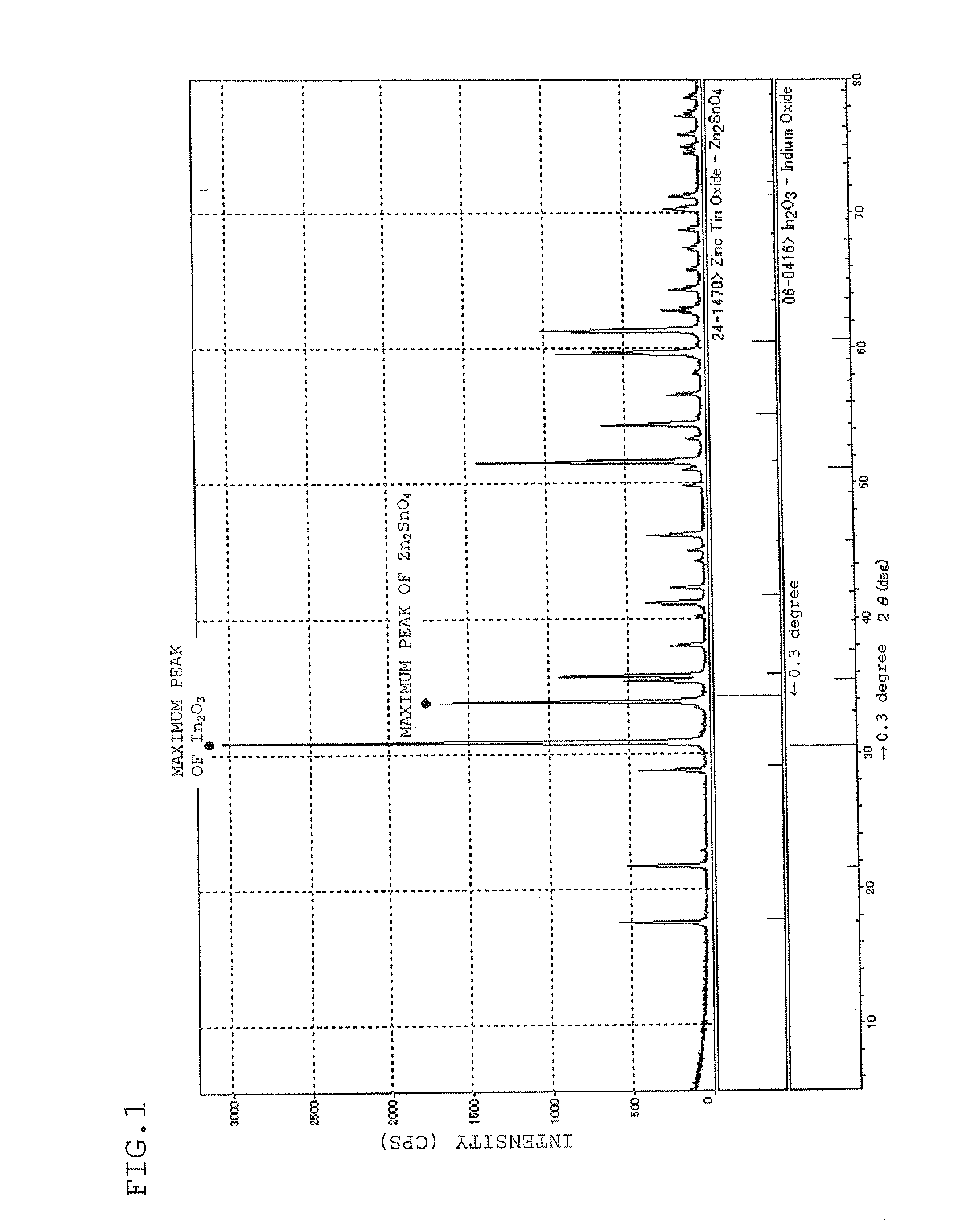
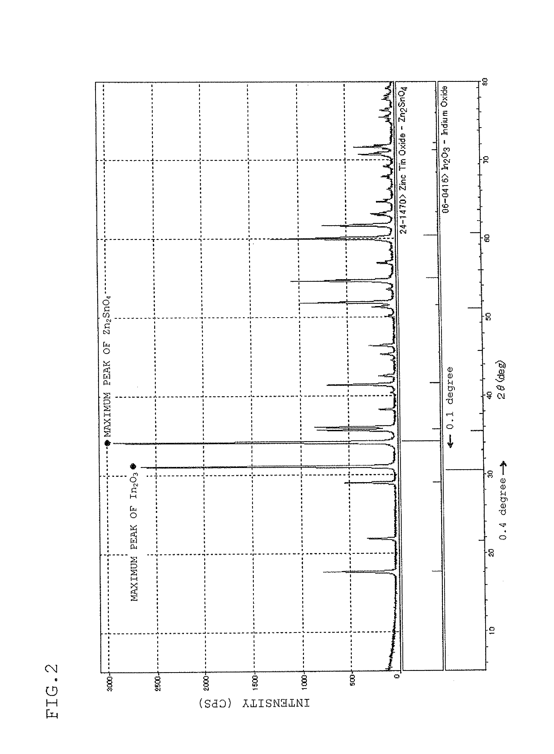
[0303]The theoretical relative d...

example 6

(1) Production of Sputtering Target

[0331]As raw materials for the target, indium oxide with a purity of 4N and an average particle diameter of 2 μm, zinc oxide with a purity of 4N and an average particle diameter of 0.6 μm, and tin oxide with a purity of 4N and an average particle diameter of 0.5 μm were mixed at atomic ratios of In / (In+Sn+Zn)=0.64, Sn / (In+Sn+Zn)=0.18, and Zn / (In+Sn+Zn)=0.18. The mixture was supplied to a wet-type ball mill and pulverized for 20 hours to obtain a raw material fine powder.

[0332]The resulting fine powder of the raw materials was granulated, and the granules were press-molded to obtain a molded article with a diameter of 10 cm and a thickness of 5 mm. The molded article was put into a firing kiln and fired at 1,400° C. under oxygen pressure for 48 hours to obtain a sintered body (target). The heating rate was 180° C. / hr and the cooling rate was 60° C. / hr.

(2) Evaluation of Target

[0333]The density, bulk resistance, X-ray diffraction analysis, crystal gra...

example 9

[0350]A large target essentially consisting of a bixbyite structure compound with the same composition as Example 6 was produced, and an electrode for a liquid crystal display for television was prepared on an organic film by DC magnetron sputtering and oxalic acid etching. A lighting test of the resulting panel prepared by using the electrode was carried out to obtain a performance comparable to a panel in which the electrode was prepared by using ITO.

[0351]No failures such as burn-in occurred during continuous lighting for 10,000 hours.


PUM

PropertyMeasurementUnit
crystal grain diameteraaaaaaaaaa
diameteraaaaaaaaaa
crystal grain diameteraaaaaaaaaa

Abstract

A sputtering target which is composed of a sintered body of an oxide which contains at least indium, tin, and zinc and includes a spinel structure compound of Zn2SnO4 and a bixbyite structure compound of In2O3. A sputtering target includes indium, tin, zinc, and oxygen with only a peak ascribed to a bixbyite structure compound being substantially observed by X-ray diffraction (XRD).

Description

TECHNICAL FIELD[0001]The present invention relates to a sputtering target prepared by sintering (hereinafter may referred to as sputtering target or as a target) and a method for preparing a sputtering target. The invention also relates to a transparent conductive film obtained by using a sputtering target, and a transparent electrode.BACKGROUND ART[0002]In recent years, development of displays has been remarkable. A liquid crystal display (LCD), an electroluminescence display (EL), a field emission display (FED), or the like is used as a display device for business machines such as a personal computer and a word processor, and a display device for control systems in factories. These displays have a sandwich structure in which a display device is held between transparent conductive oxides.[0003]A main stream material for such a transparent conductive oxide is indium tin oxide (hereinafter may abbreviated as “ITO”) prepared by a sputtering method, an ion plating method, or a vapor de...

Claims


Application Information

Patent Timeline
Patent Type & Authority Applications(United States)
IPC IPC(8): H01B5/00C23C14/34B22F3/12H01B13/00H01B1/02
CPCC04B35/453C04B35/457C04B35/6261C04B2235/32C04B2235/3232C04B2235/3241C04B2235/3272C04B2235/3281C04B2235/3284C04B2235/3286C04B2235/3293C04B2235/3418C04B2235/5445C04B2235/656C04B2235/6562C04B2235/6567C04B2235/664C04B2235/72C04B2235/763C04B2235/77C04B2235/786C04B2235/80C04B2235/96C23C14/086C23C14/3414H01B1/02H01B13/00Y10T428/24777C03C17/3644C03C2217/94C03C2218/33C03C2218/34C23C14/08C23C14/34
Inventor YANO, KOKIINOUE, KAZUYOSHITANAKA, NOBUOTANAKA, TOKIEKAIJO, AKIRAUMENO, SATOSHI
Owner IDEMITSU KOSAN CO LTD
Why Eureka
Try Eureka