

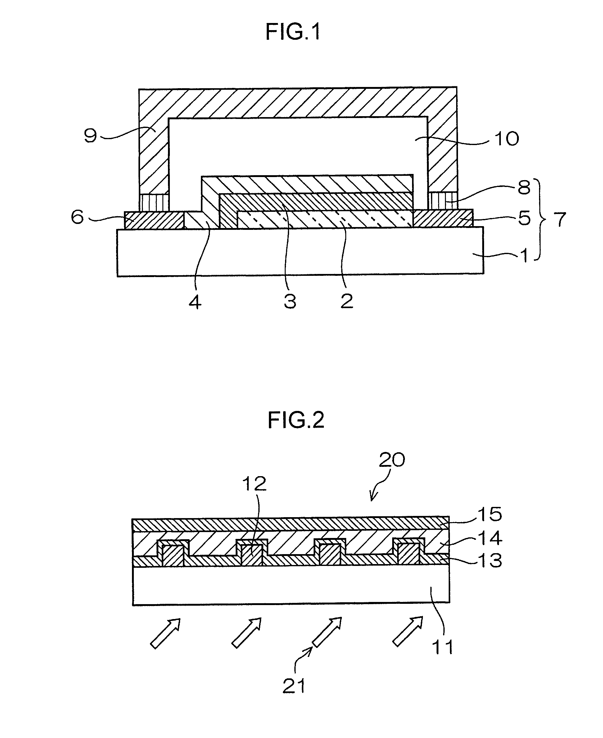
Charge transport film, method for producing the same, and light-emitting element and photoelectric conversion element using the same
a charge transport film and charge technology, applied in the direction of sustainable manufacturing/processing, final product manufacturing, conductors, etc., can solve the problems of long time, similar problems, and difficult to obtain uniform thin films without defects, and achieve excellent charge transportability, excellent durability, and excellent performance.
- Summary
- Abstract
- Description
- Claims
- Application Information
AI Technical Summary
Benefits of technology
Problems solved by technology
Method used
Image

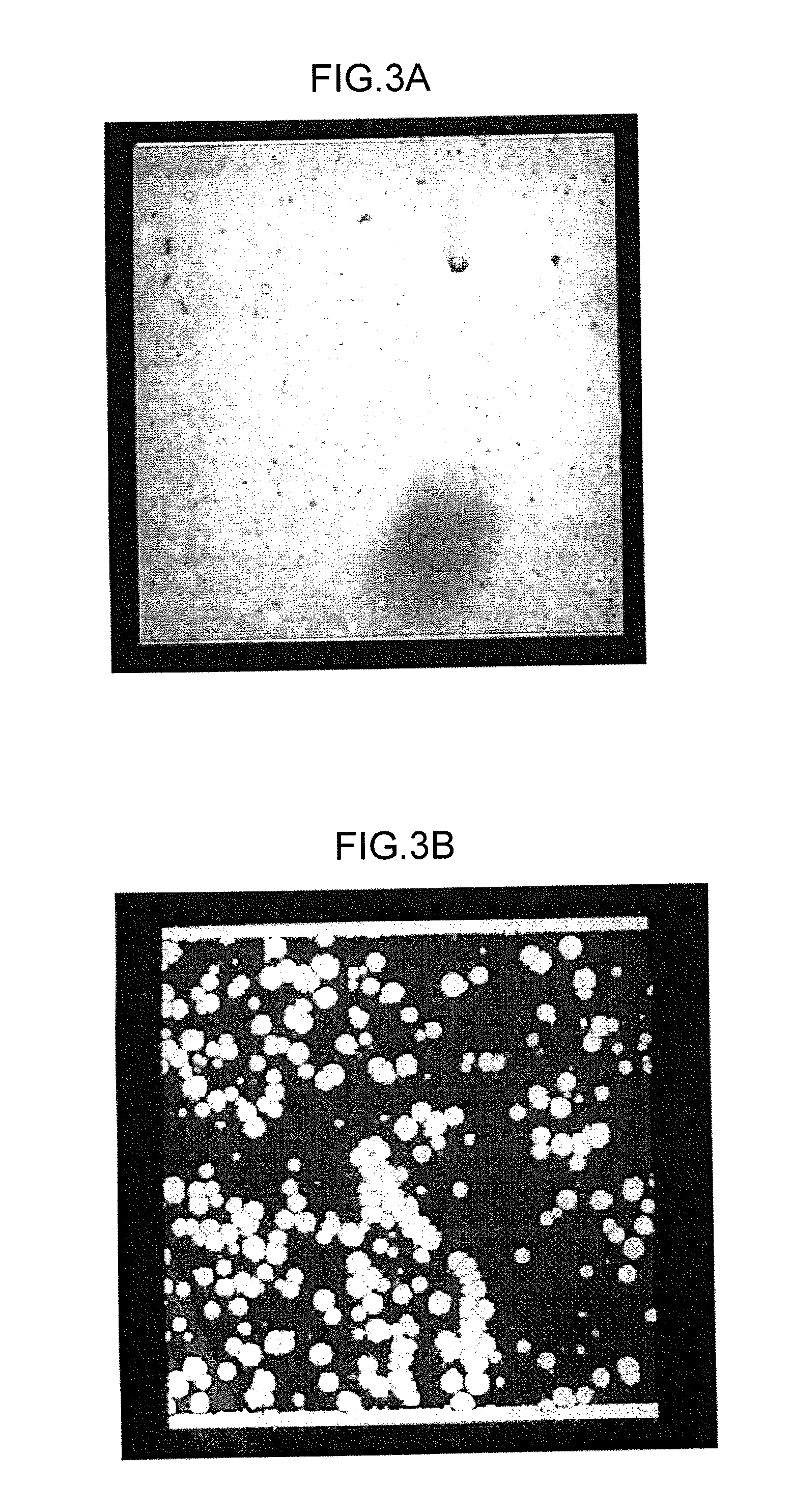
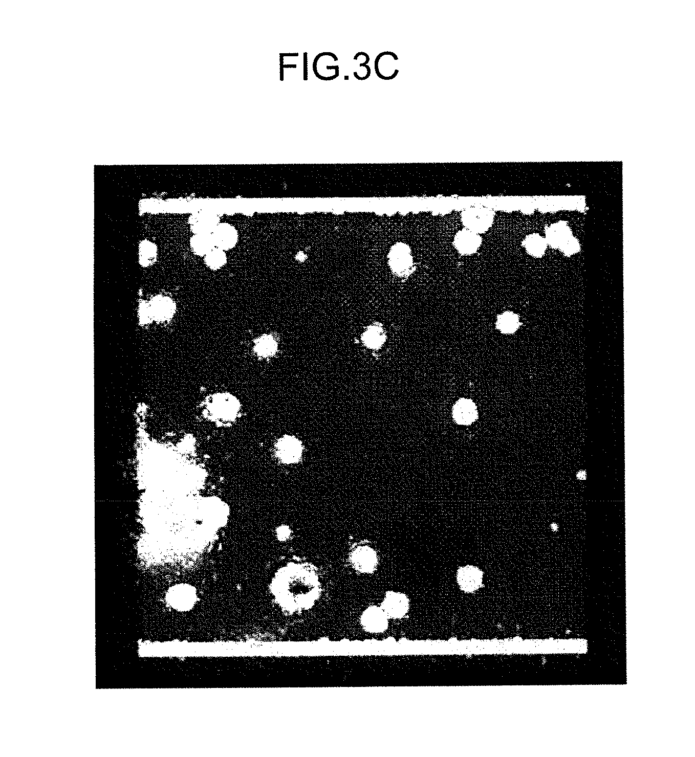
Examples
example 1
[0222]
[0223](Preparation of Coating Liquid A for Forming Hole Injection Layer)
[0224]1% by mass of compound A which is a tetrafunctional acrylate compound [having the structure shown below: which corresponds to the exemplary compound (H-29) described above], 0.25% by mass of PC-Z type polycarbonate (trade name: PANLIGHT TS-2020, manufactured by Teijin Chemicals Ltd.) and 98.75% by mass of a solvent [a solvent prepared by mixing tetrahydrofuran (hereinafter, described as THF) and xylene at a mass ratio of THF / xylene=70 / 30] were mixed to prepare a coating liquid A for forming a hole injection layer.
[0225](Preparation of Organic EL Element)
[0226]ITO (indium tin oxide) was deposited at a thickness of 150 nm on a glass substrate having a size of 25 mm×25 mm×0.7 mm, to prepare a transparent supporting substrate. This transparent supporting substrate was subjected to etching and then subjected to washing, thereby obtaining an ITO glass substrate.
[0227]Onto the ITO glass substrate thus obtai...
synthesis example 1
Synthesis of Compound 1
[0245]4-(benzyloxy)benzoic acid (20.0 g, 87.6 mmol), 4-(hexyloxy)phenol (17.0 g, 87.6 mmol), N,N′-dicyclohexylcarbodiimide (21.7 g, 105 mmol) and 4-dimethylaminopyridine (535 mg, 4.38 mmol) were dissolved in 300 mL of methylene chloride. The resulting solution was stirred for 3 hours at room temperature. Then, 300 mL of pure water was added thereto, and then the resulting liquid was filtered to remove insoluble matters. Thereafter, the obtained solution was subjected to separation operation, and the resulting methylene chloride solution was washed with a saturated aqueous sodium chloride solution and dried over magnesium sulfate. After methylene chloride was distilled off, the resulting solid matter was washed with methanol. Thereby, a white solid compound, 4-(hexyloxy)phenyl 4-(benzyloxy)benzoate (24.9 g) was obtained.
[0246]The 4-(hexyloxy)phenyl 4-(benzyloxy)benzoate obtained as described above (5.0 g, 12.4 mmol) and palladium on carbon (2.5 g in the wet sta...
synthesis example 2
Synthesis of Compound 2
[0248]Compound 2 (having the structure shown below) was obtained in a manner substantially similar to that in the above Synthesis Example 1, except that 4-(pentyl)phenol and 4-(tosyloxy)butyl acrylate were used respectively instead of 4-(hexyloxy)phenol and acryloyl chloride used in the Synthesis Example 1.
PUM
| Property | Measurement | Unit |
|---|---|---|
| Tg | aaaaa | aaaaa |
| charge transport | aaaaa | aaaaa |
| charge transporting | aaaaa | aaaaa |
Abstract
Description
Claims
Application Information