
N-Doped Semiconducting Material Comprising Phosphine Oxide Matrix and Metal Dopant

a technology of phosphine oxide and metal dopant, which is applied in the direction of organic semiconductor devices, organic chemistry, group 5/15 element organic compounds, etc., can solve the problems of high vacuum conditions, high cost, and difficult handling

Pending Publication Date: 2016-11-03
NOVALED GMBH
View PDF10 Cites 20 Cited by
  • Summary
  • Abstract
  • Description
  • Claims
  • Application Information

AI Technical Summary

Benefits of technology

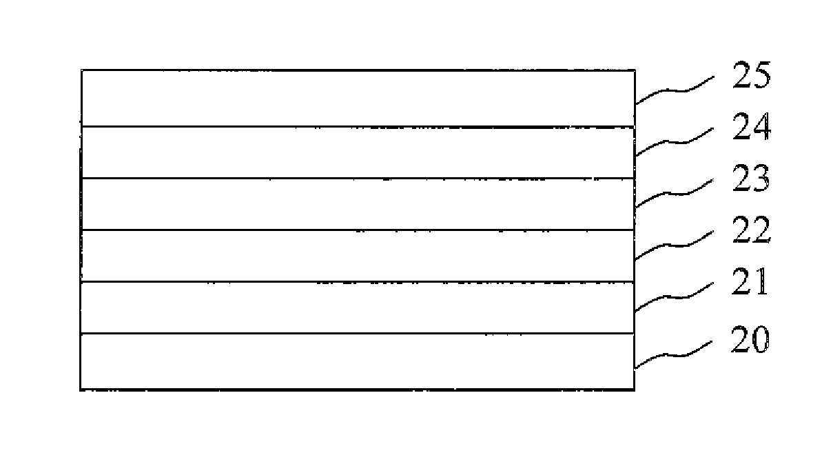
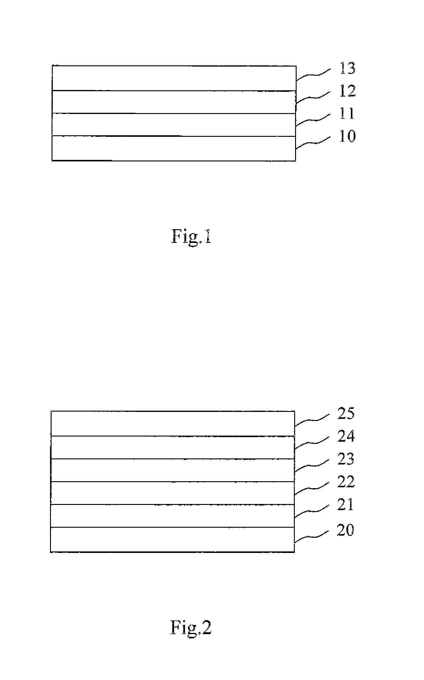
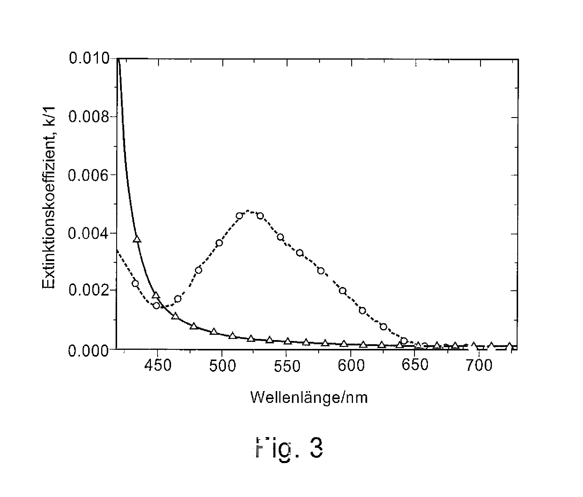
This patent describes the benefits of using special materials in electronic devices. These materials have been tested and compared to other materials known in the art. The results show that the inventive combination of materials and dopants works better than other combinations. This patent provides a detailed description of the devices used in the testing.

Problems solved by technology

First, it is very reactive, moisture and highly air sensitive material that renders any handling difficult and incurs significant additional costs for mitigating the high safety and fire hazard unavoidably linked with its use.
Second, its quite low normal boiling point (678° C.) indicates that it may be highly volatile under high vacuum conditions.
Taking into account that the evaporation temperatures for typical matrix compounds used in organic semiconducting materials at pressures below 10−3 Pa are typically between 150-400° C., avoiding an uncontrolled caesium evaporation, resulting in its undesired deposition contaminating the colder parts of the whole equipment (e.g. the parts that are shielded against heat radiation from the organic matrix evaporation source), is a really challenging task.
Such technical solution was provided e.g. in WO 2007 / 065685, however, it does not solve the problem of caesium high volatility.
Yet, all these alloys are still highly air and moisture sensitive.
Moreover, this solution has further drawback in the fact that the vapour pressure over the alloy changes with the decreasing caesium concentration during the evaporation.
That creates new problem of an appropriate deposition rate control, e.g. by programming the temperature of the evaporation source.
So far, quality assurance (QA) concerns regarding robustness of such process on an industrial scale hamper a wider application of this technical solution in mass production processes.
Its main disadvantage is their high price caused by relative chemical complexity of comprised ligands and necessity of a multistep synthesis of the final complex, as well as additional costs incurred by necessity of using the protective shells and / or by the QA and logistic issues linked with shell recycling and refilling.
Providing organic n-dopants or n-dopant precursors with such long-term thermal stability is a real technical challenge so far.
Moreover, the complicated arrangement of the production equipment that must ensure a defined and reproducible additional energy supply for achieving reproducibly the desired doping level (through the in situ activation of the dopant precursor deposited in the matrix) represents an additional technical challenge and a potential source of additional CA issues in mass production.
This process is, however, hardly applicable in contemporary industrial VTE sources, due to difficult control of such decomposition reaction in a larger scale.
Moreover, release of nitrogen gas as a by-product in this reaction brings a high risk that especially at higher deposition rates desired in the mass production, the expanding gas will expel solid caesium azide particles from the evaporation source, causing thus high defect counts in the deposited layers of doped semiconducting materials.
The main disadvantage of metals salt dopants is that they improve basically only electron injection to the adjacent layers and do not increase the conductivity of doped layers.
Their utilization for decreasing the operational voltage in electronic devices is thus limited on quite thin electron injecting or electron transporting layers and does hardly allow e.g. an optical cavity tuning by using ETLs thicker than approximately 25 nm, what is well possible with redox-doped ETLs having high conductivity.
Furthermore, metal salts typically fail as electrical dopants in cases wherein creation of new charge callers in the doped layer is crucial, e.g. in charge generating layers (CGL, called also p-n junctions) that are necessary for the function of tandem OLEDs.
Moreover, if Li is co-evaporated with matrix compounds that have evaporation temperatures in the range 150-300° C., its significantly higher evaporation temperature in comparison with the matrix evaporation temperature already causes cross-contamination problems in the VTE equipment.
Unfortunately, not only in these two documents cited here as examples but throughout the scientific and patent literature overall, there is in fact lack of any evidence that some of these suggestions have ever been experimentally tested.
The coordinatively unsaturated iron compound then reacts with the matrix, what results in the observed doping effects.
On the other hand, the authors of the present application confirmed in a screening done with dozens of state-of-the-art ETMs that Mg does not possess a sufficient doping strength for usual ETMs.

Method used


Image

  • N-Doped Semiconducting Material Comprising Phosphine Oxide Matrix and Metal Dopant
  • N-Doped Semiconducting Material Comprising Phosphine Oxide Matrix and Metal Dopant
  • N-Doped Semiconducting Material Comprising Phosphine Oxide Matrix and Metal Dopant

Examples


synthesis examples

[0121]The synthesis of phosphine oxide ETL matrix compounds is well described in many publications, besides the literature cited at particular compounds listed above and describing typical multistep procedures used for these compounds, the compound E6 was prepared, according to Bull. Chem. Soc. Jpn., 76, 1233-1244 (2003), quite specifically by an anionic rearrangement of the compound E2.

[0122]For the new compounds, however, the typical procedures were used, as exemplified below specifically for the compounds E5 and E8. All synthesis steps were carried out under argon atmosphere. Commercial materials were used without additional purification. Solvents were dried by appropriate means and deaerated by saturation with argon.

synthesis example 1

[1,1′:4′,1″-terphenyl]-3,5-diylbis-diphenylphosphine oxide E5

Step 1: 3,5-dibromo-1,1′:4′,1″-terphenyl

[0123]

[0124]All components (10.00 g (1.0 eq, 50.50 mmol) [1,1′-biphenyl]-4-yl-boronic acid, 23.85 g (1.5 eq, 75.75 mmol) 1,3,5-tribromobenzene, 1.17 g (2.0 mol %, 1.01 mmol) tetrakis(triphenyl phosphine)palladium(0), 10.70 g (2 eq, 101 mmol) sodium carbonate in 50 mL water, 100 mL ethanol and 310 mL toluene) were mixed together and stirred at reflux for 21 hours. The reaction mixture was cooled to room temperature and diluted with 200 mL toluene (three layers appear). The aqueous layer was extracted with 100 mL toluene, the combined organic layers were washed with 200 mL water, dried and evaporated to dryness. The crude material was purified via column chromatography (SiO2, hexane / DCM 4:1 v / v) The combined fractions were evaporated, suspended in hexane and filtered off to give 9.4 g of a white glittering solid (yield 48%, HPLC purity 99.79%).

Step 2: [1,1′:4′,1″-terphenyl]-3,5-diylbis...

synthesis example 2

(9,9-dihexyl-9H-fluorene-2,7-diyl)bis-diphenylphosphine oxide E8

[0128]

[0129]2,7-Dibromo-9,9-dihexylfluorene (5.00 g, 1.0 eq, 10.2 mmol) was placed in a flask and deaerated with argon. Then anhydrous THF (70 mL) was added, and the mixture was cooled to −78° C. 9.7 mL (2.5M solution in hexanes, 2.4 ea, 24.4 mmol) n-butyllithium were then added dropwise; the resulting solution was stirred for 1 h at −78° C., and then progressively warmed to −50° C. After slow addition of pure chlorodiphenylphosphine (4.0 mL, 2.2 eq, 22.4 mmol), the mixture was left to stir overnight till room temperature. MeOH (20 mL) was added to quench the reaction, and the solution was evaporated to dryness. The solid was re-dissolved in DCM (50 mL), H2O2 (30 wt % aqueous solution, 15 mL) was added dropwise, and the mixture left under stirring. After 24 h, the organic phase was separated, washed subsequently with water and brine, dried over MgSO4, and evaporated to dryness. Purification by chromatography (silica, gr...


PUM

PropertyMeasurementUnit
Nanoscale particle sizeaaaaaaaaaa
Boiling pointaaaaaaaaaa

Abstract

The present invention relates to an electrically doped semiconducting material comprising at least one metallic element as n-dopant and at least one electron transport matrix compound comprising at least one phosphine oxide group, a process for its preparation, and an electronic device comprising the electrically doped semiconducting material.

Description

[0001]The present invention concerns organic semiconducting material with improved electrical properties, process for its preparation, electronic device utilizing the improved electrical properties of the inventive semiconducting material, particularly the device comprising this organic semiconducting material in an electron transporting and / or electron injecting layer, and electron transport matrix compound applicable in semiconducting material of present invention.I. BACKGROUND OF THE INVENTION[0002]Among the electronic devices comprising at least a part based on material provided by organic chemistry, organic light emitting diodes (OLEDs) have a prominent position. Since the demonstration of efficient OLEDs by Tang et al. in 1987 (C. W. Tang et al., Appl. Phys. Lett. 51 (12), 913 (1987)), OLEDs developed from promising candidates to high-end commercial displays. An OLED comprises a sequence of thin layers substantially made of organic materials. The layers typically have a thickn...

Claims


Application Information

Patent Timeline
IPC IPC(8): H01L51/00H01L51/56C07F9/53H01L51/50
CPCH01L51/005H01L51/5076H01L51/56H01L2251/301C07F9/5329H01L51/0052H01L51/002C08K5/5397C07F9/5728C07F9/64C07F9/65522C07F9/65527C07F9/65583C07F9/58H10K59/32H10K71/30H10K85/60H10K50/165H10K71/00H10K71/164H10K85/615H10K2102/00
Inventor FADHEL, OMRANEROTHE, CARSTENBIRNSTOCK, JANWERNER, ANSGARGILGE, KAIANGERMANN, JENSZOLLNER, MIKEBLOOM, FRANCISCOROSENOW, THOMASCANZLER, TOBIASKALISZ, TOMASDENKER, ULRICH
Owner NOVALED GMBH
Learn More