Microwave dielectric component and manufacturing method thereof
- Summary
- Abstract
- Description
- Claims
- Application Information
AI Technical Summary
Benefits of technology
Problems solved by technology
Method used
Image

Examples
first embodiment
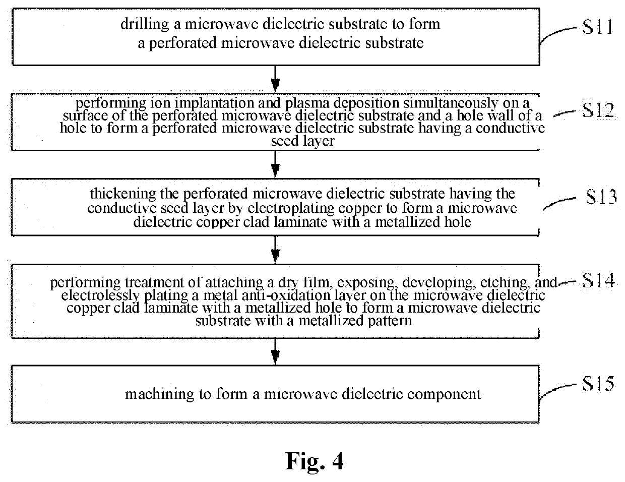
[0092]FIG. 4 shows a flow chart of a method of manufacturing a microwave dielectric component in accordance with the present invention. The method of manufacturing a microwave dielectric component comprises the following steps:
Step S11: drilling a microwave dielectric substrate to form a perforated microwave dielectric substrate;
Step S12: performing ion implantation and plasma deposition simultaneously on a surface of the perforated microwave dielectric substrate and a hole wall of the hole to form a perforated microwave dielectric substrate having a conductive seed layer;
Step S13: thickening the perforated microwave dielectric substrate having the conductive seed layer by electroplating copper to form a microwave dielectric copper clad laminate with a metallized hole;
Step S14: performing treatment of attaching a dry film, exposing, developing, etching, and electrolessly plating a metal anti-oxidation layer on the microwave dielectric copper clad laminate with the metallized hole to...
second embodiment
[0094]FIG. 5 shows a flow chart of a method of manufacturing a microwave dielectric component in accordance with the present invention. The method of manufacturing a microwave dielectric component comprises the following steps:
Step S21: cutting a microwave dielectric substrate to form a perforated microwave dielectric substrate;
Step S22: performing ion implantation and plasma deposition treatment simultaneously on the surface of the microwave dielectric substrate and the hole wall to form a perforated microwave dielectric substrate having a conductive seed layer;
Step S23: thickening the perforated microwave dielectric substrate having the conductive seed layer by electroplating copper to form a copper-clad microwave dielectric substrate with a metallized hole;
Step S24: performing treatment of attaching a dry film, exposing, developing, etching, and plating a metal anti-oxidation layer on the copper-clad microwave dielectric substrate with the metallized hole to form a metal conducti...
third embodiment
[0096]FIG. 6 shows a flow chart of a method of manufacturing a microwave dielectric component in accordance with the present invention. The method of manufacturing a microwave dielectric component comprises the following steps:
Step S31: drilling a microwave dielectric substrate to form a perforated microwave dielectric substrate;
Step S32: performing ion implantation and plasma deposition on the perforated microwave dielectric substrate to form a perforated microwave dielectric substrate having a conductive seed layer;
Step S33: thickening the perforated microwave dielectric substrate having the conductive seed layer by electroplating copper and electroplating a metal anti-oxidation layer to form a microwave dielectric copper clad laminate with a metallized hole; and
Step S34: machining the microwave dielectric copper clad laminate with the metallized hole to form a microwave dielectric component.
[0097]The electroplated copper thickening of the microwave dielectric component formed by ...
PUM
| Property | Measurement | Unit |
|---|---|---|
| Thickness | aaaaa | aaaaa |
| Thickness | aaaaa | aaaaa |
| Diameter | aaaaa | aaaaa |
Abstract
Description
Claims
Application Information
 - R&D Engineer
- R&D Manager
- IP Professional
- Industry Leading Data Capabilities
- Powerful AI technology
- Patent DNA Extraction
Browse by: Latest US Patents, China's latest patents, Technical Efficacy Thesaurus, Application Domain, Technology Topic.
© 2024 PatSnap. All rights reserved.Legal|Privacy policy|Modern Slavery Act Transparency Statement|Sitemap