

Planarization composition for removing metal films
- Summary
- Abstract
- Description
- Claims
- Application Information
AI Technical Summary
Benefits of technology
Problems solved by technology
Method used
Image

Examples
example 1
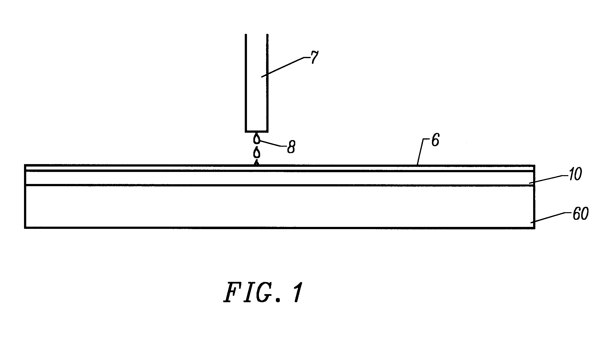
A planarization composition is formed using an ethyl silicate slurry having a content by weight percent of the following components:
The pH of the ethyl silicate slurry was approximately 12.0 and the particle size was 188 nm + / -13.5%. Ferric Nitrate and nitric acid are added to the ethyl silicate slurry in a volumetric ration of 4:1:4. The resultant planarizing composition set forth above is placed between a pad and the surface coating having the following composition:
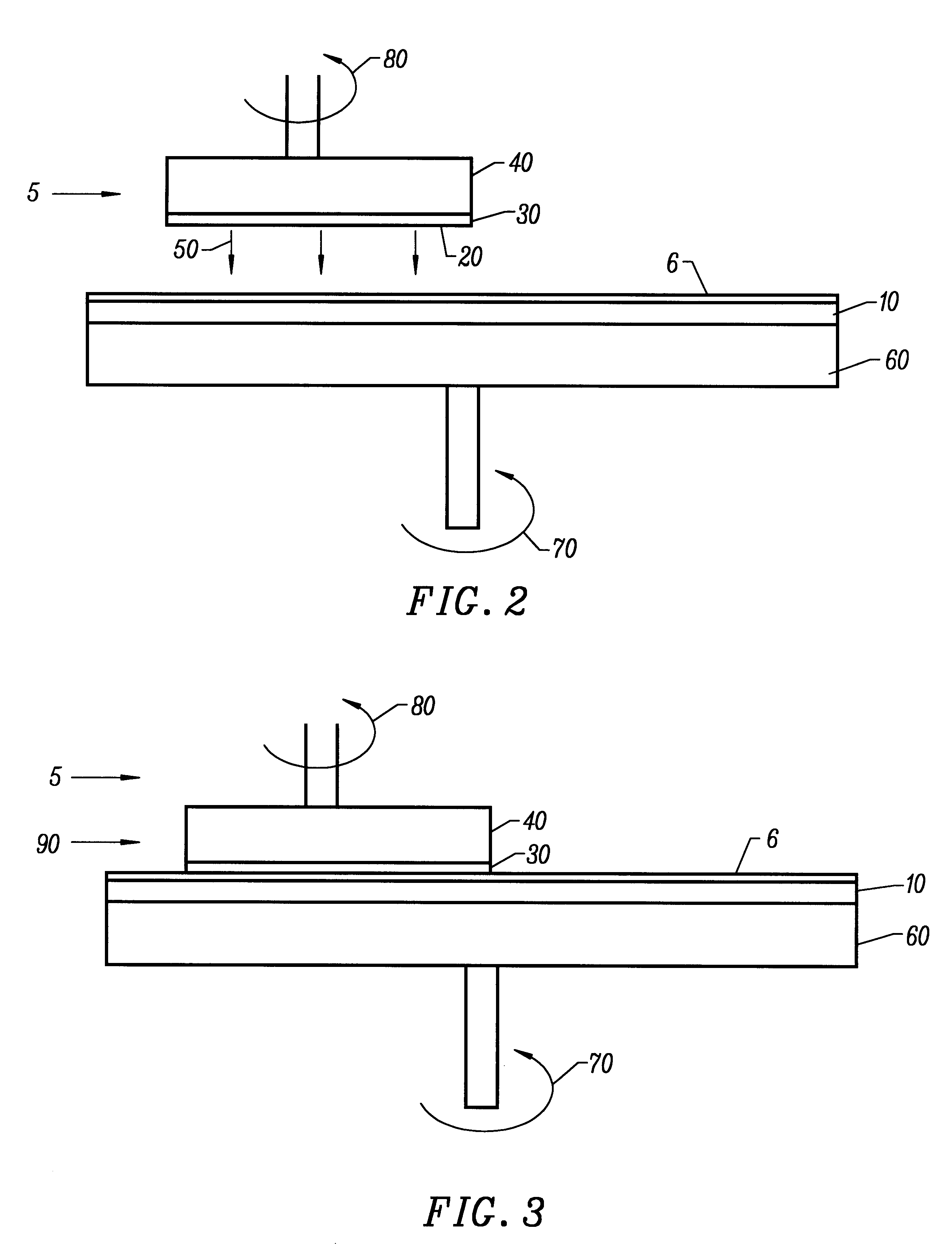
The polishing pad was a Thomas West TWI C-22 pad. The example comprises positioning the planarizing composition set forth above between a pad and the surface coating and rubbing the pad against the surface coating according to the following planarizing parameters:
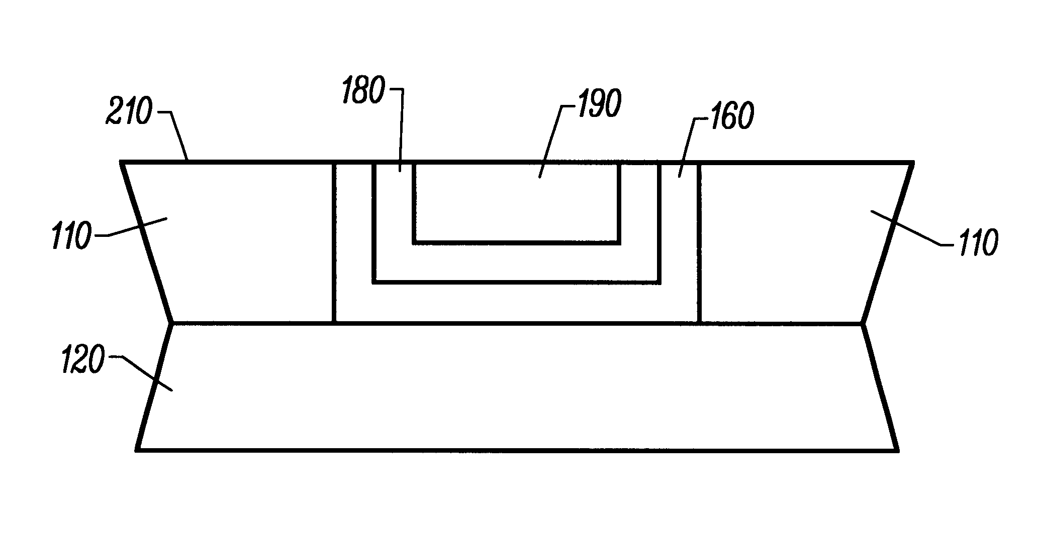
Within a 120 second planarizing period, all surface coatings totaling 7,000 angstroms were cleared to the underlying LPCVD oxide. The measured planarization rate was calculated to be 5,823 angstroms per minute. The tungsten, titanium nitride and titanium filled...
example 2
A planarization composition is formed using an ethyl silicate slurry having a content by weight percent of the following components:
The pH of the ethyl silicate slurry was approximately 12.1 and the particle size was 323+ / -20.0%. Hydrogen Peroxide and Acetic Acid are added to the ethyl silicate slurry in a volumetric ration of 2:1:1. The resultant planarizing composition set forth above between a pad and the surface coating having the following composition:
The polishing pad was a Rodel Suba-500 pad. The example comprises positioning the planarizing composition set forth above between a pad and the surface coating and rubbing the pad against the surface coating according to the following planarizing parameters:
Within a 120 second planarizing period, all surface coatings totaling 7,000 angstroms were cleared to the underlying LPCVD oxide. The measured planarizing rate was calculated to be 2,430 angstroms per minute. The within wafer nonuniformity was + / -3.5%. The tungsten, titanium ni...
example 3
A planarization composition is formed using an ethyl silicate slurry having a content by weight percent f the following components:
The pH of the ethyl silicate slurry was approximately 12.1 and the particle size was 188+ / -13.5%. Hydrogen Peroxide and Acetic Acid are added to the ethyl silicate slurry in a volumetric ratio of 1:1:1. The resultant planarizing composition set forth above was between a pad and the surface coating having the following composition:
The polishing pad was a Rodel IC1000-2A pad. The example comprises positioning the planarizing composition set forth above between a pad and the surface coating and rubbing the pad against the surface coating according to the following planarizing parameters:
The measured planarization rate was calculated to be 3,469 angstroms per minute. The within wafer on uniformity was 1.0%. The selectivity of the tungsten / titanium nitride / titanium surface coating during the planarization process was measured to be 1:1:1.
A secondary planariza...
PUM
 Abstract
Description
Claims
Application Information