Process for the formation of silicon oxide films

a technology of silicon oxide and film, applied in the direction of liquid/solution decomposition chemical coating, electric/magnetic/electromagnetic heating, nuclear engineering, etc., can solve the problems of low productivity, low production yield, and inability to easily apply to a substra

Inactive Publication Date: 2003-02-11
JSR CORPORATIOON
View PDF8 Cites 50 Cited by
  • Summary
  • Abstract
  • Description
  • Claims
  • Application Information

AI Technical Summary

Problems solved by technology

However, of these processes, the above dry processes to form a silicon oxide film have the following problems; that is, (a) since it is a gas phase reaction, the generation of particles of impurities in a gas phase causes the contamination of an apparatus or the inclusion of foreign matters, thereby causing low production yield, (b) since the material is in gaseous form, it is difficult to form a film having a uniform thickness on a substrate whose surface is not smooth, (c) productivity is low because the formation of the film is slow, (d) complicated and expensive radio-frequency generator and vacuum apparatus are required in the case of plasma CVD, and (e) they cannot be easily applied to a substrate having a large area.
Further, in these dry processes, since gaseous silicon hydride which is highly toxic and highly reactive is used as the material, it not only is difficult to handle but also requires a sealed vacuum apparatus since it is in gaseous form.
In general, these apparatus not only are bulky and expensive but also consume a large amount of energy in a vacuum or plasma system, causing an increase in product cost.
Thus, since water is produced as the reaction proceeds, a compact silicon oxide film cannot be easily obtained, and cracks are liable to be produced due to the occurrence of theinternal stress of the film.
Further, since the sol-gel reaction requires a high temperatures heating, the process cannot be applied to a plastic substrate having low heat resistance.
This process, however, has a point to be improved, which is low productivity caused by a large amount of ultraviolet light required to oxidize and decompose the organic component.
When less than 5 silicon atoms are present, the silicon compound itself becomes unstable due to the distortion of the ring and difficult to handle.
On the other hand, when more than 20 silicon atoms are present, a decrease in solubility attributed to the cohesion of the silicon compound can be recognized, whereby the number of solvents that can be selected becomes smaller disadvantageously.

Method used


Image

  • Process for the formation of silicon oxide films
  • Process for the formation of silicon oxide films
  • Process for the formation of silicon oxide films

Examples


synthesis example 1

The inside of a 2-liter four-neck flask equipped with a thermometer, a condenser, a dropping funnel and an agitator was substituted with an argon gas, 1.5 liters of dried tetrahydrofuran and 27.4 g of metal lithium were then charged into the flask, and the content of the flask was bubbled with an argon gas. While this suspension was cooled with ice under agitation, 500 g of diphenyldichlorosilane was added through the dropping funnel. The reaction was continued until the metal lithium completely disappeared. Thereafter, the reaction mixture was poured into ice water to precipitate the reaction product. This precipitate was separated by filtration and washed fully with water and then with cyclohexane. Further, this crude product was recrystallized from ethyl acetate to give 216 g of undecaphenylcyclohexasilane. Its structure was checked by TOF-MS, NMR and IR. Then, 200 g of dodecaphenylcyclohexasilane and 2,500 ml of toluene were charged into a 1-liter flask, 5 g of aluminum chloride...

synthesis example 2

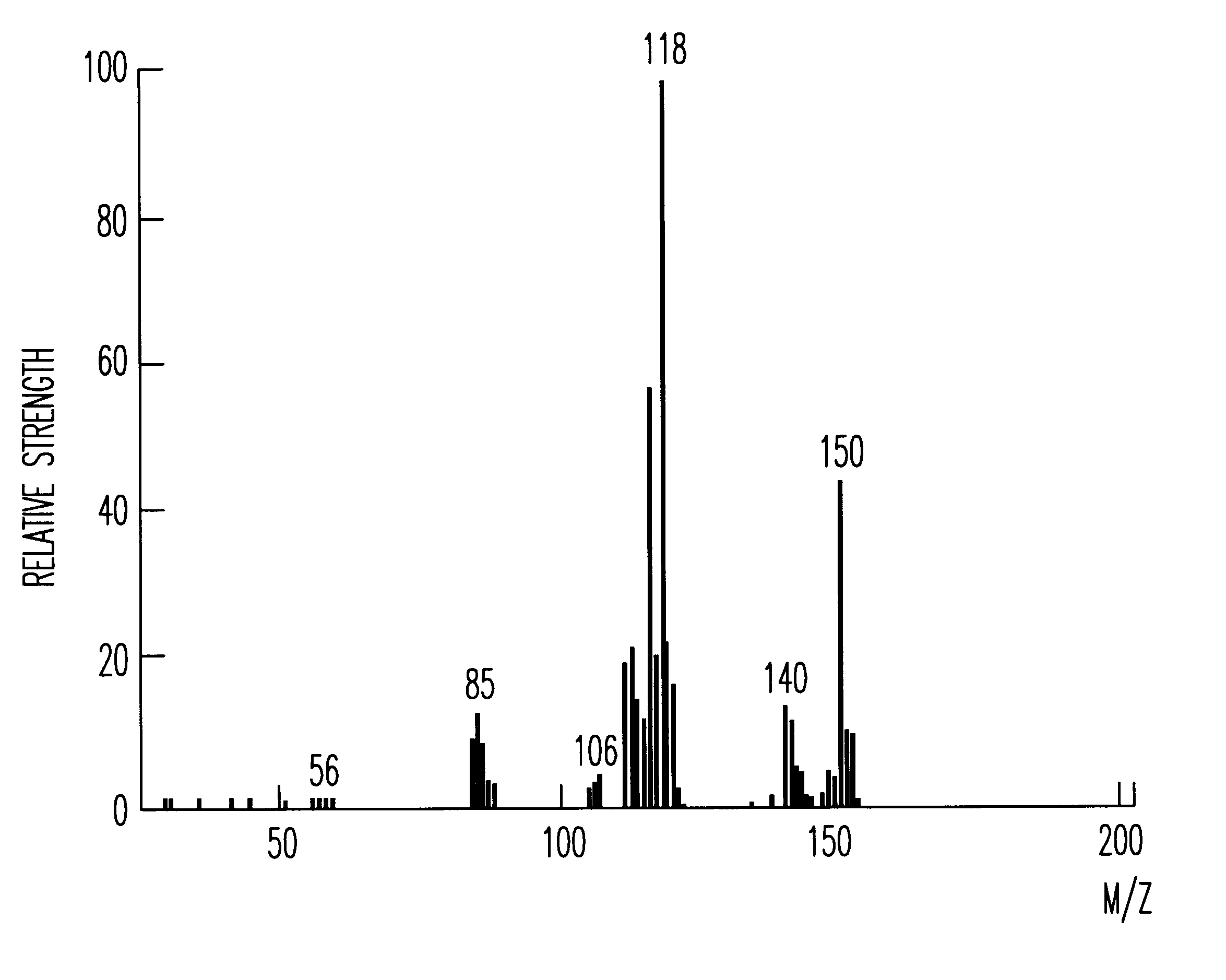
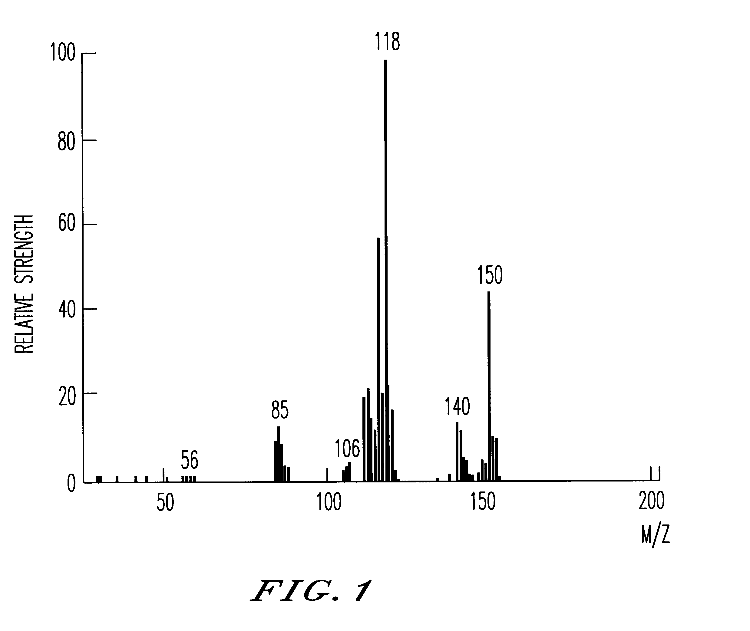
The recrystallization mother liquor of the dodecaphenylcyclohexasilane of Synthesis Example 1 was further purified by the method of chromatography to give 55 g of decaphenylcyclopentasilane as a side product. Using this side product, 25 g of decachloropentasilane was obtained under the same reaction condition as in Synthesis Example 1. The decachloropentasilane was reduced to give 6 g of cyclopentasilane(Si.sub.5 H.sub.10). The production thereof was checked by MS, .sup.29 Si--NMR and IR spectra. The MS spectrum thereof is shown in FIG. 1.

synthesis example 3

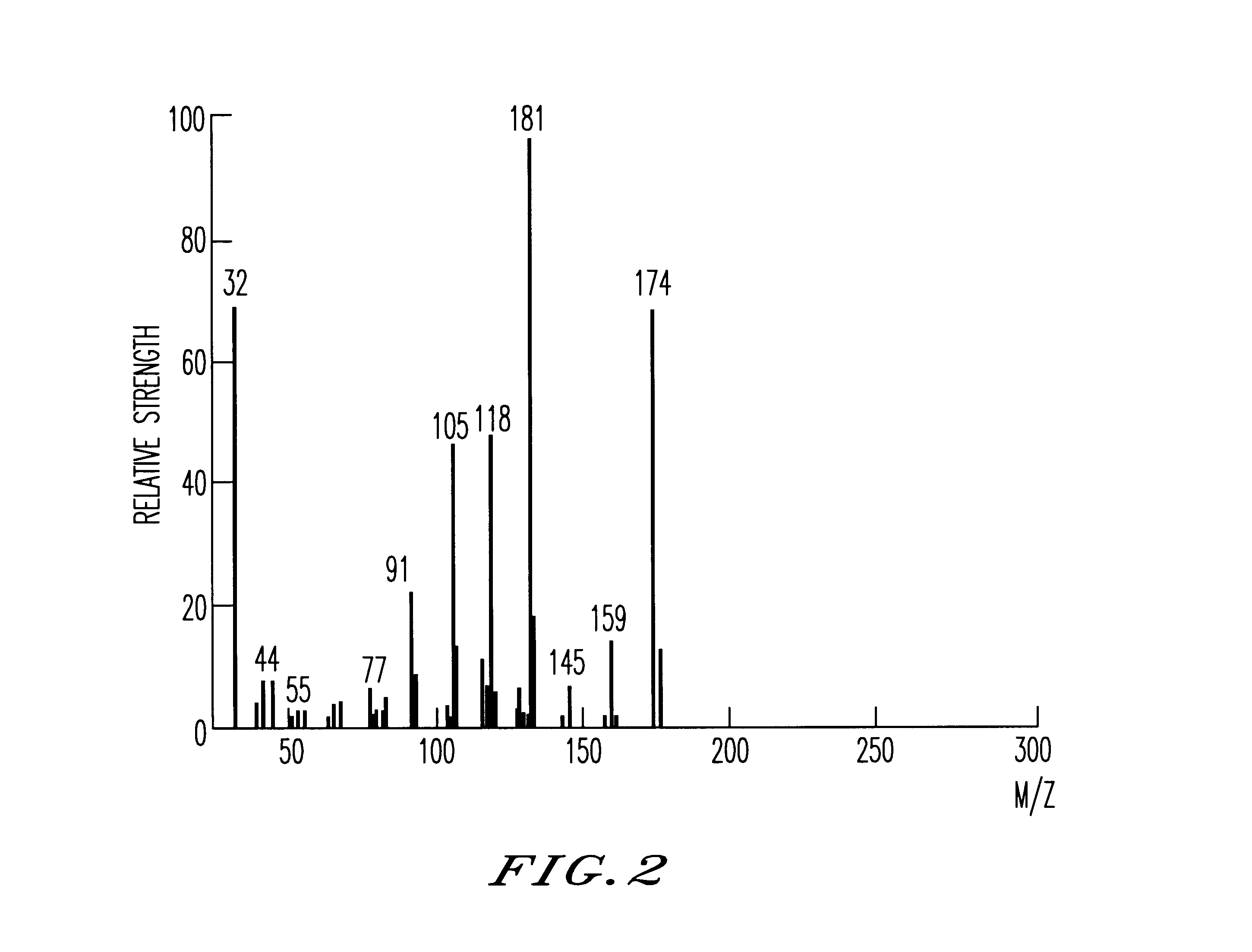
The inside of a 3-liter four-neck flask equipped with a thermometer, a condenser, a dropping funnel and an agitator was substituted with an argon gas, 2 liters of dried tetrahydrofuran and 75 g of metal lithium were then charged into the flask, and the content of the flask was bubbled with an argon gas. While this suspension was agitated at 0.degree. C., 500 g of phenyltrichlorosilane was added through the dropping funnel. The reaction was continued at 0.degree. C. until the metal lithium completely disappeared and, thereafter, the content of the flask was further agitated at room temperature for 12 hours. The dark-brown reaction mixture was poured into ice water to precipitate the reaction product. This precipitate was separated by filtration, washed fully with water and vacuum dried to give 210 g of a phenyl group-containing polycyclic silicon compound. A hundred fifty grams of the phenyl group-containing polysilane compound was caused to be suspended in 2 liters of toluene, 5 g o...


PUM

PropertyMeasurementUnit
temperaturesaaaaaaaaaa
thicknessaaaaaaaaaa

Abstract

There is provided a process for forming a silicon oxide film which is useful as an electrical insulating film, dielectric film or protective film as used in LSI, thin-film transistor, photoelectric converter, photosensitive body and the like. The process comprises forming a coating film from a polysilane compound represented by the formula SinRm (wherein n is an integer of 3 or more, m is an integer of n to 2n+2, and a plurality of R's are independently a hydrogen atom or an alkyl group) and oxidizing the coating film to form the silicon oxide film.

Description

The present invention relates to a process for forming a silicon oxide film. More specifically, it relates to a process for forming a silicon oxide film which is useful as an electrical insulating film, dielectric film or protective film as used in LSI, thin-film transistor, photoelectric converter, photosensitive body and the like.PRIOR ARTSHeretofore, a silicon oxide film has been frequently used as an electrical insulating film, dielectric film or protective film in silicon devices including a semiconductor. In general, as processes for forming these silicon oxide films, there have been known dry processes such as one comprising thermal oxidizing silicon in the air, one comprising forming the film by plasma CVD using a silane gas or a disilane gas in an oxidizing gas such as oxygen or nitric oxide, and one comprising forming the film directly from quartz by sputtering; and wet processes such as one comprising coating alkoxysilane such as tetraethoxysilane in a partially hydrolyze...

Claims


Application Information

Patent Timeline
Patent Type & Authority Patents(United States)
IPC IPC(8): C23C18/12C23C18/00H01L21/02H01L21/316H01L21/312
CPCC23C18/1212C23C18/122C23C18/1279H01L21/316H01L21/3121C23C18/14H01L21/3122H01L21/02236H01L21/02211H01L21/02282H01L21/02164H01L21/02323H01L21/02318C23C18/143C23C18/145H01L21/324H01L21/02337H01L21/02345
Inventor MATSUKI, YASUO
Owner JSR CORPORATIOON
Why Eureka
Try Eureka