Silicon nitride powder, silicon nitride sintered body, sintered silicon nitride substrate, and circuit board and thermoelectric module comprising such sintered silicon nitride substrate

a technology of silicon nitride and silicon nitride, which is applied in the field of silicon nitride powder, silicon nitride sintered body, sintered silicon nitride substrate, and circuit board and thermoelectric module comprising such, can solve the problems of mechanical strength, substrate unit cracking, and decrease in mounting reliability

Inactive Publication Date: 2005-01-25
HITACHI METALS LTD
View PDF18 Cites 89 Cited by
  • Summary
  • Abstract
  • Description
  • Claims
  • Application Information

AI Technical Summary

Benefits of technology

Accordingly, an object of the present invention is to provide a high-thermal conductivity, silicon nitride sintered body excellent in mechanical strength and free from anisotropic thermal conductivity, without costly high-temperature, high-pressure, anisotropic sintering.
Not only because large pores and roughness are likely to be formed on a surface of the silicon nitride green body, but because large pores and roughness are likely to be formed by reaction with an atmosphere so gas during the sintering process of a green body, the as-sintered surface of the silicon nitride sintered body generally has as large pores and roughness as about 50 μm or more. Such large pores and roughness function as sites of stress concentration, and the larger the pores and roughness, the likelier the cracking occurs at low stress. It has been found that by removing an as-sintered surface layer containing large pores and roughness from the silicon nitride substrate, it is possible to suppress cracking due to thermal stress in bonding interfaces between the silicon nitride substrate and the electrodes. In view of this, using as a substrate a silicon nitride sintered body, from which an as-sintered surface layer having large pores and roughness are removed by grinding, it has been found that circuit boards and thermoelectric modules in which cracking occurs less likely from the substrate can be obtained.

Problems solved by technology

Though aluminum nitride substrates have already been used as such ceramic substrates, the aluminum nitride substrates lack mechanical strength, fracture toughness, etc., resulting in the likelihood that substrate units are cracked by fastening at an assembling step.
Also, because a circuit board comprising silicon semiconductor chips mounted onto an aluminum nitride substrate is likely to be cracked by thermal cycles because of large difference in a thermal expansion coefficient between silicon chips and an aluminum nitride substrate, the aluminum nitride substrate is cracked by thermal cycles, resulting in decrease in mounting reliability.
Therefore, special high-temperature, high-pressure apparatuses such as hot pressing or HIP, etc. are needed, resulting in increase in the costs of the sintered bodies.
Also, because they need a complicated molding process for producing green bodies with oriented silicon nitride grains, the productivity is inevitably extremely low.
However, because this method uses large amounts of Y2O3 and SiO2 as a slug, the resultant treated powder is so aggregated that it should be crushed in a grinding machine, etc.
Also, because it is necessary to carry out an acid treatment for removing oxides from the surfaces of silicon nitride grains and a classification treatment for controlling a particle size, the processes are complicated.
This reference describes that when the oxygen content as converted to SiO2 is less than 2 weight % in the starting silicon nitride powder, the β-particle ratio of the silicon nitride powder is insufficient and likely to be ununiform, and that when the oxygen content exceeds 5 weight % as converted to SiO2, SiO2 remains in the heat-treated silicon nitride powder, resulting in poor properties.
Also, this method is disadvantageous in that SiO2 powder is added in advance to control the oxygen content of the starting material powder, and that the heat treatment should be carried out in an oxygen atmosphere.
It is further disadvantageous in that because the resultant silicon nitride powder is aggregated by the heat treatment, the silicon nitride powder should be crushed by a ball mill, a roll crusher, etc.
However, a high-temperature, high-pressure apparatus is needed to obtain the above high-thermal conductivity, silicon nitride sintered body, resulting in increase in its production cost.
Further, because heat treatment is carried out after sintering, the productivity is extremely low.
In addition, detailed composition analysis and observation are not conducted on the precipitation phase in the silicon nitride grains in the above sintered body, failing to make clear correlations with improvement in thermal conductivity.
However, the above references concerning the circuit board fail to investigate a surface condition of the silicon nitride substrate dominating the bonding of a circuit plate of copper or aluminum to the silicon nitride substrate.
In any of the above bonding methods, without adjusting the surface condition or texture of the silicon nitride substrate, there is large unevenness in the bonding strength of the metal circuit plate to the silicon nitride substrate and the thermal cycle resistance of the resultant circuit board, failing to provide a high-reliability circuit board.
However, Japanese Patent Laid-Open No 11-349381 fails to describe technologies necessary for enhancing the reliability of the thermoelectric module and thus stabilizing its operation.
When voltage is applied to the terminals of a thermoelectric module comprising an insulating silicon nitride substrate, peeling has undesirably occurred at bonding interfaces between the insulating silicon nitride substrate and the electrodes.

Method used


Image

  • Silicon nitride powder, silicon nitride sintered body, sintered silicon nitride substrate, and circuit board and thermoelectric module comprising such sintered silicon nitride substrate
  • Silicon nitride powder, silicon nitride sintered body, sintered silicon nitride substrate, and circuit board and thermoelectric module comprising such sintered silicon nitride substrate
  • Silicon nitride powder, silicon nitride sintered body, sintered silicon nitride substrate, and circuit board and thermoelectric module comprising such sintered silicon nitride substrate

Examples


example 1

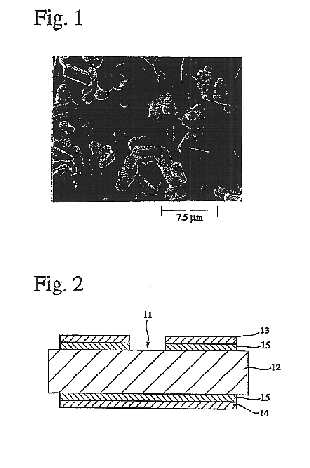
Silicon nitride powder formed by an imide decomposition method and having an oxygen content of less than 1.0 weight % as converted to SiO2 and an average particle size of 0.2-2.0 μm was charged into a crucible made of BN, heat-treated at 1,400° C.-1,950° C. for 1-20 hours in an N2 atmosphere of normal pressure to 1.0 MPa (10 atm), and then cooled to room temperature to form a first silicon nitride powder. The production conditions of each sample are shown in Table 1 on the columns of Sample Nos. 1-11, and the β-particle ratio, oxygen content, impurities (Fe, Al), average particle size and aspect ratio of each first silicon nitride powder are shown in Table 2 on the columns of Sample Nos. 1-11.

The impurities (Fe, Al) in the first silicon nitride powder were analyzed by inductively coupled plasma emission spectroscopy (ICP) method. The oxygen content of the first silicon nitride powder was measured by an infrared thermal absorption method. The β-particle ratio of the first silicon nit...

example 2

Added to 10 weight % of the first silicon nitride powder having a β-particle ratio of 30% or more, which was produced in the same manner as in EXAMPLE 1, and 86 weight % of α-silicon nitride powder were 3 weight % of MgO and 1 weight % of Y2O3 as sintering aids to form a mixed powder. The resultant mixed powder was charged into a resin ball-milling pot filled with a solution of a 2-weight-% amine dispersant in toluene / butanol together with silicon nitride balls as a pulverization medium, and mixed for 48 hours. 15 parts by weight of a polyvinyl-type, organic binder and 5 parts by weight of a plasticizer (dimethyl phthalate) were added to 100 parts by weight of the mixed powder in the pot and mixed for 48 hours to form a slurry. This slurry was cast to a green sheet by a doctor blade method. By heating the resultant green sheet at 400-600° C. for 2-5 hours in the air, the organic binder was removed.

The degreased green body was sintered at 1,850° C. and 0.9 MPa (9 atm) for 5 hours in ...

example 3

Added to 10 weight % of the first silicon nitride powder having a β-particle ratio of 30% or more, which was produced in the same manner as in EXAMPLE 1, and 86 weight % of α-silicon nitride powder were 1 weight % of MgO and 3 weight % of Gd2O3 as sintering aids to form a mixed powder. The mixed powder was charged into a ball-milling pot filled with ethanol containing 2 weight % of a dispersant (Leogard GP), and mixed. The resultant mixture was vacuum-dried and granulated through a 150-μm-opening sieve. It was then CIP-molded at a pressure of 3 tons by a press apparatus to form disc-shaped green bodies of 20 mm in diameter and 10 mm in thickness and those of 100 mm in diameter and 15 mm in thickness. Each of the resultant green bodies was sintered at a temperature of 1,850° C.-1,950° C. and a pressure of 0.7-0.9 MPa (7 atm-9 atm) for 5-40 hours in a nitrogen gas atmosphere. The production conditions of the first silicon nitride powder are shown in Table 5, the properties of the resu...


PUM

PropertyMeasurementUnit
particle sizeaaaaaaaaaa
surface roughness Raaaaaaaaaaa
densityaaaaaaaaaa

Abstract

A silicon nitride sintered body comprising Mg and at least one rare earth element selected from the group consisting of La, Y, Gd and Yb, the total oxide-converted content of the above elements being 0.6-7 weight %, with Mg converted to MgO and rare earth elements converted to rare earth oxides RExOy. The silicon nitride sintered body is produced by mixing 1-50 parts by weight of a first silicon nitride powder having a particle ratio of 30-100%, an oxygen content of 0.5 weight % or less, an average particle size of 0.2-10 μm, and an aspect ratio of 10 or less, with 99−50 parts by weight of α-silicon nitride powder having an average particle size of 0.2-4 μm; and sintering the resultant mixture at a temperature of 1,800° C. or higher and pressure of 5 atm or more in a nitrogen atmosphere.

Description

FIELD OF THE INVENTIONThe present invention relates to a high-strength, high-thermal conductivity, silicon nitride sintered body suitable for semiconductor substrates and electronics parts for heat sinks for power modules, heat-generating components, and structural members for general machines, members for molten metals or members for thermal engines, etc., to a method for producing such a silicon nitride sintered body, to silicon nitride powder used for the production of such a silicon nitride sintered body and a method for producing it, and further to a circuit board and a thermoelectric element module respectively comprising a sintered silicon nitride substrate.PRIOR ARTBecause a silicon nitride sintered body is excellent in mechanical properties such as high-temperature strength properties and wear resistance, etc., heat resistance, low thermal expansion, thermal shock resistance and corrosion resistance to molten metals, it has conventionally been used for various structural ap...

Claims


Application Information

Patent Timeline
Patent Type & Authority Patents(United States)
IPC IPC(8): C04B35/584C04B35/593C01B21/00C01B21/068H01L23/373H01L23/12H01L23/15H01L23/34H05K1/03
CPCC01B21/068C04B35/5935H01L23/15H01L23/3731H05K1/0306C01B21/0687Y10T428/266C01P2004/03C01P2004/54C01P2004/61C01P2004/62C01P2006/12C01P2006/80H05K2201/0355Y10S428/901H01L2924/0002Y10T428/26Y10T428/31Y10T428/252Y10T428/24917H01L2924/00
Inventor IMAMURA, HISAYUKIHAMAYOSHI, SHIGEYUKIKAWATA, TSUNEHIROSOBUE, MASAHISA
Owner HITACHI METALS LTD
Why Eureka
Try Eureka