Apparatus for inspection with electron beam, method for operating same, and method for manufacturing semiconductor device using former

a technology of electron beam and electron beam, which is applied in the direction of material analysis, instruments, and optical methods using wave/particle radiation, etc. it can solve the problems of low inspection speed, high cost of inspection apparatus, and inferior inspection apparatus of electron beam method in view of throughput, so as to prevent the accuracy of defect detection from being deteriorated and achieve higher accuracy

Inactive Publication Date: 2005-02-15
EBARA CORP
View PDF13 Cites 100 Cited by
  • Summary
  • Abstract
  • Description
  • Claims
  • Application Information

AI Technical Summary

Benefits of technology

According to this aspect, the image obtaining means obtains respective images for the plurality of regions to be inspected which have been displaced one from another while being superimposed partially one on another, and the defect determination means determines the defect in the sample by comparing the obtained images for the plurality of regions to be inspected with the reference image which has been stored in advance. In this way, since the present invention allows a plurality of images to be taken for the inspection regions of different positions, the inspection images not being offset a lot from the reference image can be selectively used in the following processes so as to prevent the defect detecting accuracy from being deteriorated by the position mismatching. Besides, even if the sample and the image obtaining means have been brought in such a physical relationship that the inspection pattern could partially fall out of the image region to be inspected, there shoul

Problems solved by technology

The inspection apparatus of electron beam method, however, has a weak point in that the inspection apparatus of electron beam method is inferior to the inspection apparatus of optical method in view of throughput.
However, the inspection speed (sometime also referred to as inspection speed) thereof is very low, and so the development of an inspection apparatus with higher inspection speed has been expected.
Generally, since an inspection apparatus is expensive and a throughput thereof is rather lower as compared to other processing apparatuses, therefore the inspection apparatus has been used after an important process, for example, after the process of etching, membrane deposition, CMP (Chemical-mechanical polishing) planarization or the like.
Owing to this, every time when the stage moves, there occurs such an event that the vacuum level within the chamber C is deteriorated, which disadvantageously has inhibited the processing including the aforementioned exposure, inspection and process by using the charged particle beam from being performed stably, or otherwise the sample has been contaminated.
Further, there have been such problems in the above-described stage including a combination of the hydrostatic bearing and the differential pumping mechanism that because of the differential pumping mechanism having been added, the structure has become more complicated and the reliability as a stage has decreased in contrast with the increased cost.
As for the electron beam apparatus of the image projecting method by itself, since a plurality of signals from a plurality of pixels on the sample surface can be captured all at once, therefore this method is advantageous in the point of the pattern inspection with the high throughput, while the method is problematic in the point that the sample may be charged due to a plurality of pixels being exposed to the irradiation of the electron beam all at once.
On the other hand, in the case where a mark for positioning on the wafer is to be detected during the processes, a field of view may not necessarily be such wide that would be required by the image projection in the pattern inspection but a narrower field of view may be sufficient, wherein it is rather problematic that an insufficiently small pixel size may result in an insufficient mark detection accuracy.
Besides, for the MCP, as a total output charge amount (screen current×time period) is increased over a long-time use, the MCP multiplication factor is decreased, and therefore there has been a problem in that a defective image contrast may change or deteriorate with the same MCP applied voltage upon picking up the defective images successively for a long period in the defect inspection apparat

Method used


Image

  • Apparatus for inspection with electron beam, method for operating same, and method for manufacturing semiconductor device using former
  • Apparatus for inspection with electron beam, method for operating same, and method for manufacturing semiconductor device using former
  • Apparatus for inspection with electron beam, method for operating same, and method for manufacturing semiconductor device using former

Examples


first embodiment

; a Defect Inspection System of Image Projecting Type

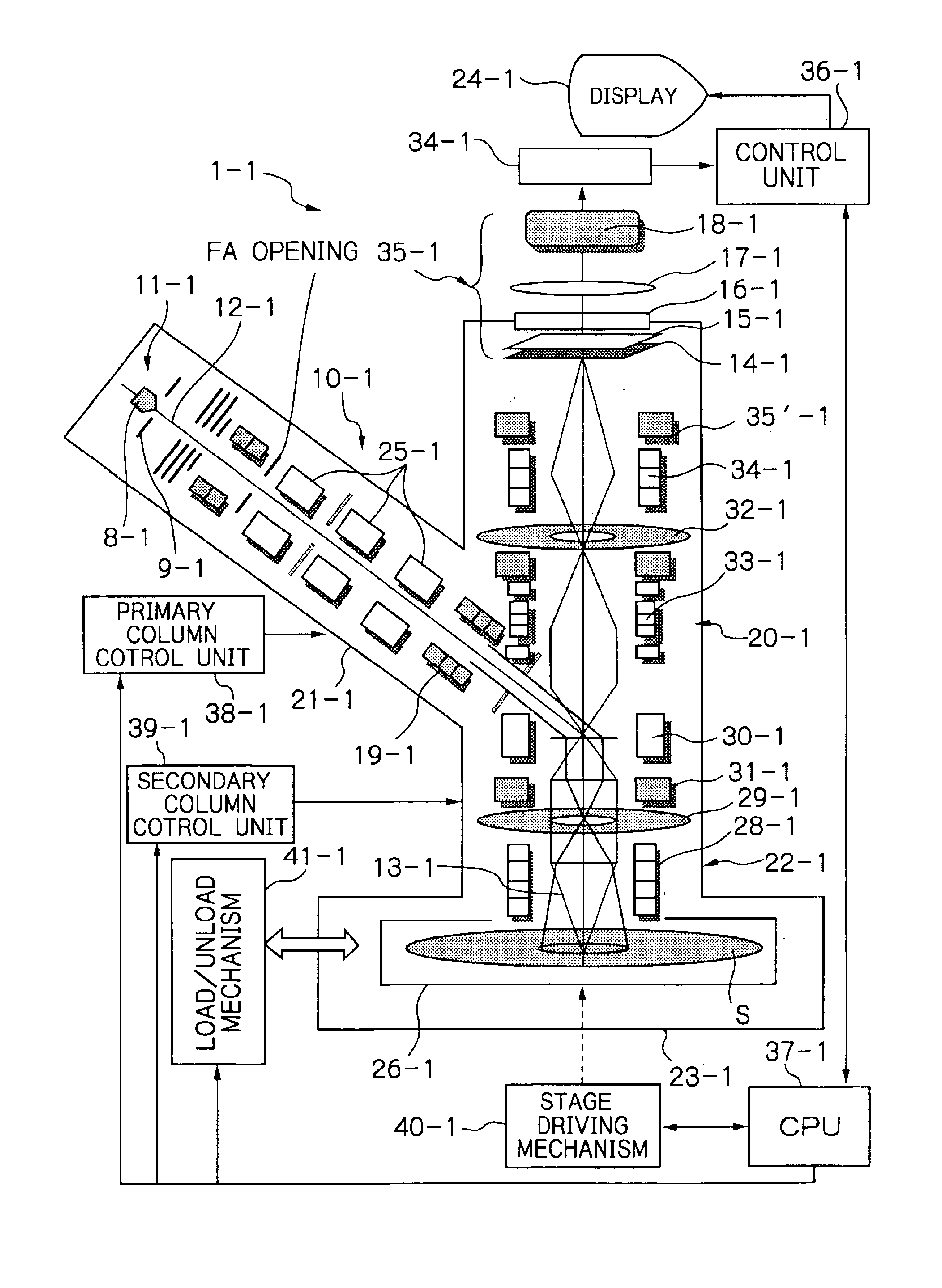
FIG. 1 shows a schematic general configuration of a defect inspection system using an electron beam apparatus 1-1 of image projecting type according to a first embodiment of the present invention. As shown in FIG. 1, the electron beam apparatus 1-1 comprises a primary column 21-1, a secondary column 22-1 and an inspection chamber 23-1. It is to be appreciated that on the purpose of this application, the context of the term “inspection” includes an evaluation apparatus for evaluating a result of the inspection.

An electron gun 11-1 comprising a cathode 8-1 and an anode 9-1 is arranged in an inside of the primary column 21-1, and an primary optical system 10-1 is arranged along an optical axis of an electron beam 12-1 (a primary electron beam) radiated from the electron gun 11-1. Further, a stage 26 is installed in an interior of the inspection chamber 23-1 and a substrate S (e.g., a wafer) as a sample is loaded on the stage 26.

The p...

second embodiment

A pattern inspection apparatus according to a second embodiment has a combination of two functions including a function for image projecting and a function as a scanning electron microscope (i.e., a function for detecting a secondary emission beam generated by scanning with a primary electron beam), in which each of these two functions can be easily switched to each other simply by an electrical operation, as will be described later.

The pattern inspection apparatus according to the second embodiment can be accomplished by employing the configuration of the electron beam apparatus 1-1 shown in FIG. 1, and further adding thereto the function as the scanning electron microscope.

The function for the image projecting is mainly used in a pattern inspection for a hardly-charged sample, while the function as the scanning electron microscope is mainly used in a pattern inspection for an easily-charged sample or in a mark detection in a registration to be preformed prior to the pattern inspec...

third embodiment

Since a defect inspection apparatus according to a third embodiment employs a defect inspection system using the electron beam apparatus 1-1 of FIG. 1, the similar numeric references are used to designate the similar components and a detailed description on the configuration of this defect inspection apparatus will be omitted.

For the MCP 14-1 of FIG. 1, it is obvious from FIG. 5, in which the operating time is represented along the lateral axis and the multiplication factor is represented along the longitudinal axis, that the multiplication factor decreases as the operating time increases. Further, it is also obvious from FIG. 6, which indicate the correlation between the voltage applied to the MCP (sometimes referred to as MCP applied voltage) and the MCP multiplication factor while representing the MCP applied voltage along the lateral axis and the MCP multiplication factor along the longitudinal axis, that the MCP multiplication factor increases in monotone up to a saturation val...


PUM


Abstract

A substrate inspection apparatus 1-1 (FIG. 1) of the present invention performs the following steps of: carrying a substrate “S” to be inspected into an inspection chamber 23-1 maintaining a vacuum in said inspection chamber; isolating said inspection chamber from a vibration; moving successively said substrate by means of a stage 26-1 with at least one degree of freedom; irradiating an electron beam having a specified width; helping said electron beam reach to a surface of said substrate via a primary electron optical system 10-1; trapping secondary electrons emitted from said substrate via a secondary electron optical system 20-1 and guiding it to a detecting system 35-1; forming a secondary electron image in an image processing system based on a detection signal of a secondary electron beam obtained by said detecting system; detecting a defective location in said substrate based on the secondary electron image formed by said image processing system; indicating and/or storing said defective location in said substrate by CPU 37-1; and taking said completely inspected substrate out of the inspection chamber. Thereby, the defect inspection on the substrate can be performed successively with high level of accuracy and efficiency as well as with higher throughput.

Description

BACKGROUND OF THE INVENTIONIn the field of semiconductor processes, the design rule is going into an age of 100 nm and the production form is on a transition from a mass production with a few models representative of a DRAM into a small-lot production with a variety of models such as a SOC (Silicon on chip). This results in an increase of a number of processes, and thus an improvement in yield for each process becomes essential, which makes more important an inspection for a defect possibly occurring in each process. The present invention relates to an apparatus to be used in the inspection of a wafer after respective processes in the semiconductor processes, and in particular to an inspection method and apparatus using an electron beam and also to a device manufacturing method using the same.In conjunction with a high integration of semiconductor device and a micro-fabrication of pattern thereof, an inspection apparatus with higher resolution and throughput has been desired. In ord...

Claims


Application Information

Patent Timeline
IPC IPC(8): G01N23/225G01N23/22H01J37/244H01J37/02H01J37/28H01J37/18H01J37/20H01J37/06H01J37/073H01J37/22G01Q30/02
CPCG01N23/225H01J37/06H01J37/073H01J37/185H01J37/20H01J37/222H01J37/244H01J37/28G01N23/2251H01J2237/2813H01J2237/082H01J2237/202H01J2237/20228H01J2237/204H01J2237/22H01J2237/24564H01J2237/2806H01J2237/2816H01J2237/2817H01L2224/48227H01L2924/01025H01L2924/01057H01L2924/01078H01L2924/3025H01L2924/01019H01L2924/01067H01L2924/10253H01J2237/2002H01J2237/0216H01J2237/2007H01L2924/00H01L2924/12032
Inventor KIMBA, TOSHIFUMISATAKE, TOHRUKARIMATA, TSUTOMUWATANABE, KENJINOJI, NOBUHARUMURAKAMI, TAKESHIHATAKEYAMA, MASAHIRONAKASUJI, MAMORUSOBUKAWA, HIROSIYOSHIKAWA, SHOJIOOWADA, SHINSAITO, MUTSUMI
Owner EBARA CORP
Why Eureka
Try Eureka