Wavelength division multiplexed optical interconnection device

a multi-wavelength, optical interconnection technology, applied in the direction of visual presentation using printers, semiconductor lasers, instruments, etc., can solve the problems of 2.5 ghz, difficult manufacturing cost, and large increase in the number of wirings, so as to facilitate implementation, improve the delay characteristics of various signals employed, and increase the data throughput of the optical interconnection device

Inactive Publication Date: 2005-06-14
HITACHI LTD
View PDF1 Cites 16 Cited by
  • Summary
  • Abstract
  • Description
  • Claims
  • Application Information

AI Technical Summary

Benefits of technology

The present invention is about a wavelength division multiplexed optical interconnection device that efficiently utilizes a semiconductor substrate with an integrated circuit being integrated thereon and lessens signal delay between input and output units. The device includes optical signal input and output units placed symmetrically on the periphery of a square main surface of the substrate. The device also integrates optical receiver and emitter driver circuits within the substrate, and uses a phase-locked loop circuit for controlling the transfer of electric signals to the optical emitter driver circuits. The device also includes a signal processing integrated circuit and a wavelength division multiplexing transmission system for achieving high-capacity and small-sized optical interconnection with effective countermeasures against noise. The device can be packaged using hybrid packaging and multi-chip integration to improve data throughput and driving band.

Problems solved by technology

However, any of the reports does not disclose one wherein laser diodes, photo diodes, their driver circuits, optical multiplexers, optical demultiplexers and an electric signal processing circuit are not brought into integration on a single semiconductor substrate.
When it is desired to increase a communication data throughput of an optical interconnection device, a restriction on the number of electric wirings connecting between optical transmitting and receiving elements and a signal processing LSI constituting the optical interconnection device, and a data band produce a bottleneck upon increase in communication capacity.
A subsequent drastic increase in the number of pins and an increase in the number of wirings are difficult in terms of the manufacturing cost.
However, a limitation on a circuit characteristic of a glass epoxy or polyimide system printed board on which elements are hybrid-packaged, is the neighborhood of 2.5 GHz.
Therefore, the method of independently packaging the various elements employed in the devices described in the first through third prior arts, hybrid-packaging them on a printed board and increasing a data throughput of each device by a multi-pin connection of high-speed wirings encounters difficulties in obtaining an optical interconnection device for transmitting high-speed signals exceeding 1 Gbit per second every signals with satisfactory reproducibility.
Further, electrical wiring connections to the signal processing LSI will produce a bottleneck and hence an increase in communication capacity is difficult as expected.
However, since the optical demultiplexer, optical multiplexer and optical waveguide are respectively comprised of the compound semiconductor, it is difficult to realize a small-sized multiplexed optical interconnection device.

Method used


Image

  • Wavelength division multiplexed optical interconnection device
  • Wavelength division multiplexed optical interconnection device
  • Wavelength division multiplexed optical interconnection device

Examples


first embodiment

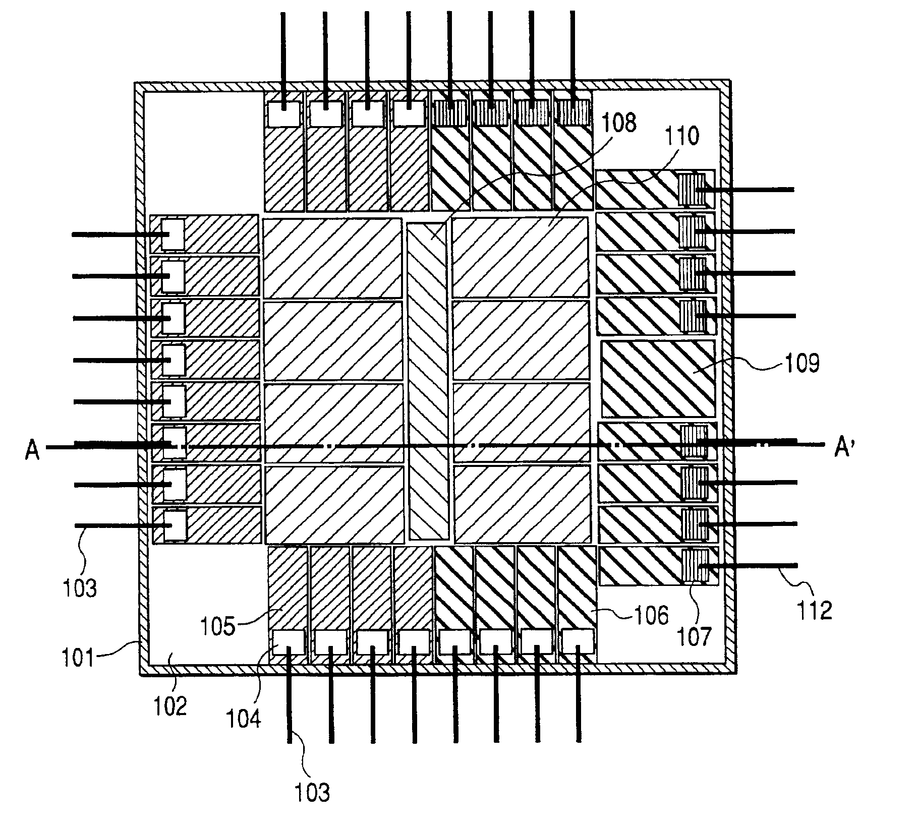
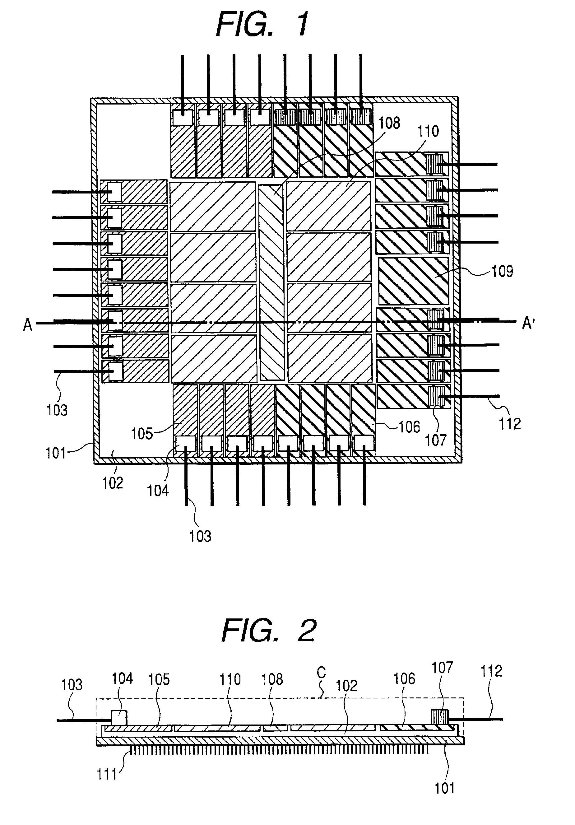
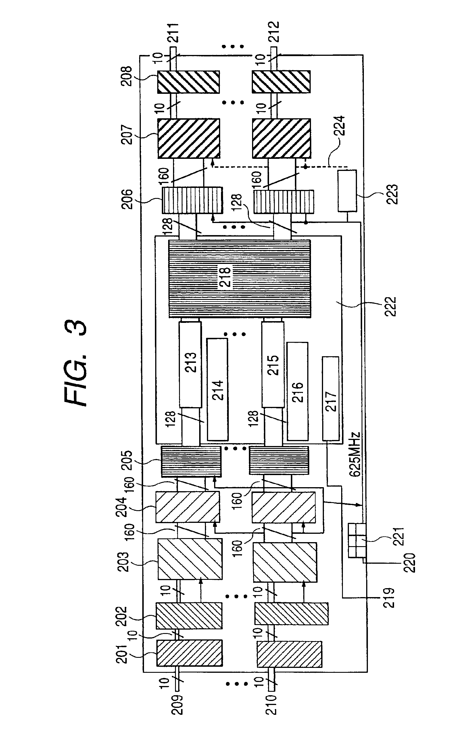
[0037]Preferred embodiments of the present invention will be described with reference to FIGS. 1 through 5. FIG. 1 is a plan view for describing a layout of an essential portion of a wavelength division multiplexed optical interconnection device according to the present invention, which is integrated on one semiconductor substrate or within one package. FIG. 2 is a cross-sectional view illustrating an essential portion taken along line A-A′ in FIG. 1. FIG. 3 is a circuit functional block diagram illustrating an essential portion which constitutes the inside of a signal processing LSI of the wavelength division multiplexed optical interconnection device, respectively. FIG. 4 is an enlarged view illustrating an essential portion of an optical input unit mounted on a printed circuit board. FIG. 5 is an enlarged view illustrating an essential portion of an optical output unit placed on the printed circuit board, respectively. Incidentally, the planes of the optical input and output unit...

second embodiment

[0063]A packing structure shown in FIG. 6 is adopted in place of the structure of the optical data input unit described in FIG. 4 in the first embodiment of the present invention. A description will be made of a second embodiment, which adopts a packing structure shown in FIG. 7 in place of the structure of the optical data output unit described in FIG. 5. The second embodiment is similar in electric circuit structure to the first embodiment. Incidentally, the planes of the optical input and output units are shown on the upper sides in FIGS. 6 and 7 and the cross-sections thereof are shown on the lower sides in FIGS. 6 and 7.

[0064]The second embodiment has a structure wherein fibers 503 and 609 and fiber receptacles 501 and 611 in which optical parallel signals are inputted and outputted from within a device, are respectively bonded to the surfaces of a mounting printed boards 513 and 613. As shown in FIG. 6, an optical single mode fiber 503 placed onto the board 513 is bent in an S...

third embodiment

[0067]A packing structure describe in FIG. 8 is adopted in place of the structure of the optical data input unit described in FIG. 4 in the first embodiment of the present invention. A description will be made of a third embodiment which adopts a packing structure described in FIG. 9 in place of the structure of the optical data output unit described in FIG. 5. Incidentally, the third embodiment is similar in electric circuit structure to the first embodiment. Incidentally, the planes of the optical input and output units are shown on the upper sides in FIGS. 8 and 9, and the cross-sections thereof are shown on the lower sides in FIGS. 8 and 9.

[0068]In the third embodiment, optical parallel signals are respectively inputted to and outputted from the device through optical fibers 702 and 801 embedded into mounting printed boards 713 and 811 without being done via fibers on the mounting printed boards. The Optical fibers 702 and 810 embedded into the boards 713 and 811 in the horizont...


PUM


Abstract

A high-speed and small-sized optical interconnection device uses wavelength-multiplexed light suitable therefor in order to make compatible between an increase in high-speed communication capacity of the optical interconnection device and an increase in high-speed communication distance thereof. A signal processing LSI is placed within a central portion of a main surface of a semiconductor substrate, and input / output units for transmitting and receiving optical wavelength-multiplexed lights are multi-chip integrated on the periphery of the main surface of the semiconductor substrate into a single package, and a wiring length can be reduced and a physical signal band for each connecting wiring can be enlarged. Further, the signal processing LSI is made up of CMOS and a driver circuit for each optical transmitting / receiving element is comprised of a Si—Ge transistor circuit, whereby a modulated signal band can be enlarged and the performance of the input / output optical signals from the device can be improved.

Description

BACKGROUND OF THE INVENTION[0001]1. Field of the Invention[0002]The present invention relates to an optical interconnection device using wavelength division multiplexed lights.[0003]2. Description of the Related Art[0004]The use of an optical interconnection device is very effective in increasing a data throughput of a data connection system lying within or between devices of a computer system and a transmission-exchanger. The term optical interconnection means communication technology wherein optical signal transfer systems comprised of optical emitters, optical receivers and optical fibers are parallel-driven to transmit signals upon short-range data communication connections within / between the devices. Through the use of the optical interconnection, high-capacity data communication connections can be implemented with a small-sized device scale and with a low delay.[0005]As examples reported up to now as to optical interconnection devices, may be mentioned, an example in which opt...

Claims


Application Information

Patent Timeline
Patent Type & Authority Patents(United States)
IPC IPC(8): G02B6/12G02B6/125G06K15/02H04N1/56H04N1/60H04N1/58G02B6/34G02B6/42G02B6/122H01L21/822H01L25/16H01L27/04H01L31/02H01L31/0232H01S5/026H01S5/40H04B10/40H04B10/50H04B10/60H04B10/80
CPCG02B6/12007G02B6/125G06K15/02H04N1/58G06K15/1852H04N1/6072G06K15/1849H01L2224/48091H01L2924/00014
Inventor NISHIMURA, SHINJI
Owner HITACHI LTD
Why Eureka
Try Eureka