

Structured organic materials and devices using low-energy particle beams
a technology of organic materials and beams, applied in the direction of discharge tubes/lamp details, thermometer details, nuclear engineering, etc., can solve the problems of serious difficulties, very fragile organic molecular crystals, and every such procedure can have a detrimental effect on device properties, etc., to achieve the effect of simplifying the patterning process, and improving the quality of organic materials
- Summary
- Abstract
- Description
- Claims
- Application Information
AI Technical Summary
Benefits of technology
Problems solved by technology
Method used
Image

Examples
example 1
Patterning of Undoped and Doped Organic Molecular Crystals
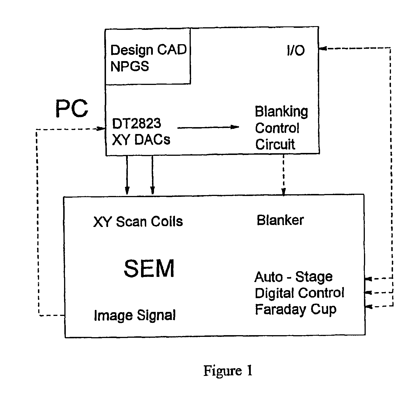
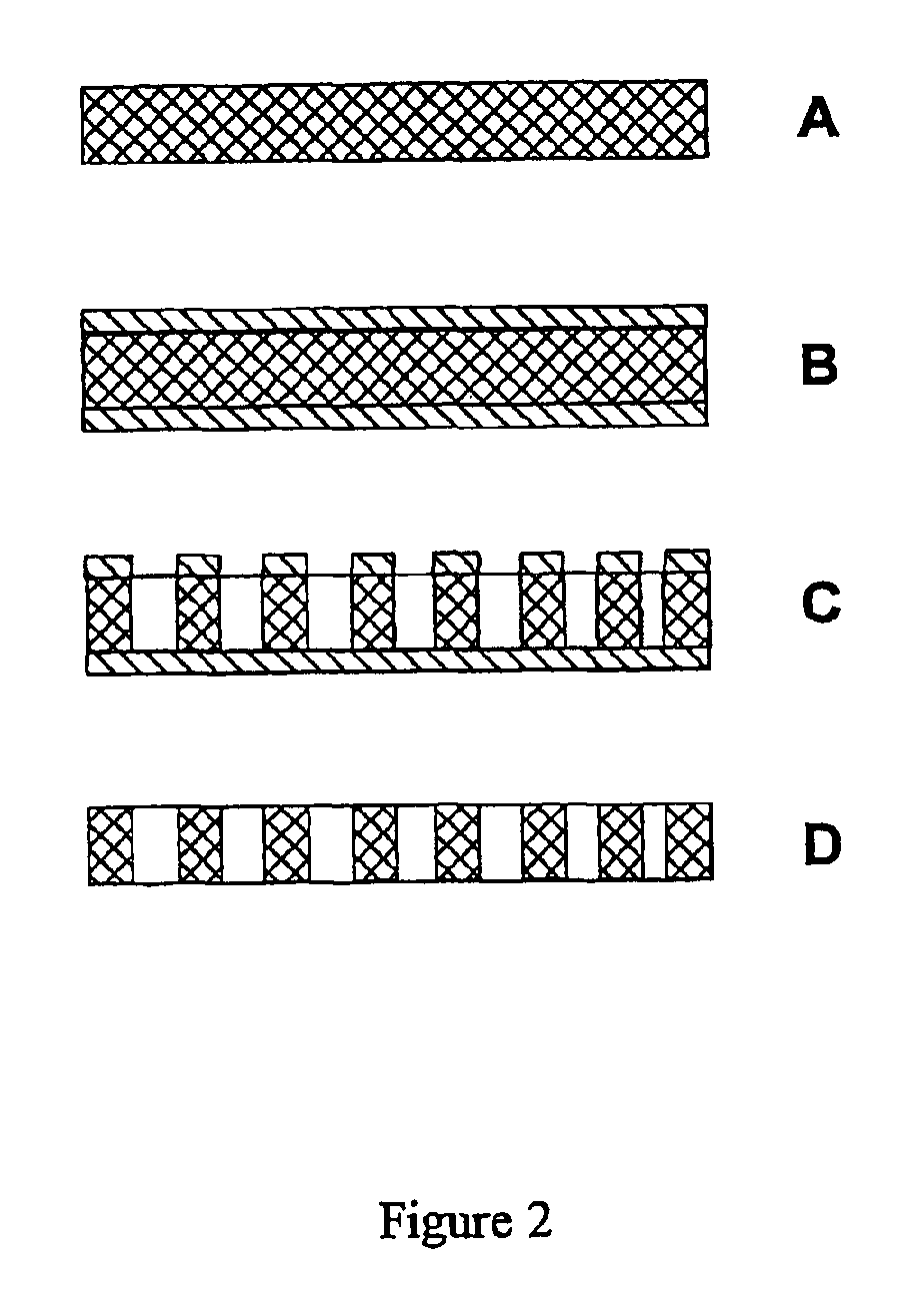
[0043]FIGS. 2A through 2D illustrate the principle of patterning undoped organic molecular crystalline or semi-crystalling material in accordance with the invention. In FIG. 2A, an organic molecular crystal thin film having a preferred thickness in the range of 0.5-20 μm is grown by physical vapor deposition. However, because the low-energy election beam with low penetration depth is used for patterning in the present invention, the method can also be applied to patterning of organic thin films grown on various substrates by vacuum thermal evaporation or by other epitaxial methods.
[0044]In FIG. 2B, the film is coated with a much thinner conducting layer of gold or aluminum by conventional sputtering or thermal deposition for the purpose of avoiding charging of the molecular crystal during patterning by the electron beam. The conducting layer is preferably on the order of ≦10 nm thick. Note that in the case of doped molecular ...
example 2
Application of the Invention for Fabrication of Organic Lasers Microdisk and Microring Lasers
[0046]Small diameter microdisks and microrings having feature sizes on the order of one micrometer are needed to fabricate a single-mode whispering-gallery-mode organic laser. FIG. 4 illustrates how such organic microstructure devices can be prepared according to the invention. An organic layer (e.g. anthracene, or tetracene) is deposited onto a gold bottom electrode layer previously deposited onto a substrate (for example, glass, Si or polymer). The microdisk (−1 μm) is formed in the organic layer according to the invention, i.e. by evaporating the organic material from around the ring. The top electrode (ITO or Al-doped ZnO) is then deposited onto the microdisk through a shadow mask, which protects other areas of the device.
Organic Distributed Bragg Reflector (DBR) Lasers
[0047]A distributed Bragg reflector (DBR) laser structure comprises an optical waveguide taking the form of a first and ...
example 4
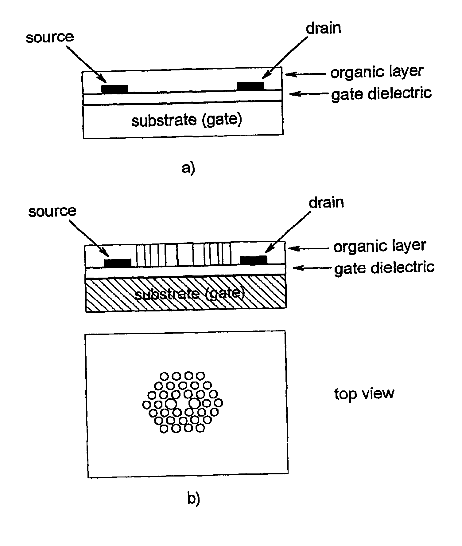
Organic Field-Effect Transistor with Imbedded 2D Photonic Crystal
[0054]Light-emitting, organic field-effect transistors are known in the art. Such a device may be improved through the invention by imbedding a two-dimensional photonic crystal with defects inside the structure. The efficiency of the laser structure with a two-dimensional photonic band-gap defect has already been demonstrated by 0. Painter et al., Science 284, 1819-1821 (1999). A light-emitting organic field elect transistor is fabricated by conventional technology (FIG. 7a). The thickness of the active area of structure should be half wavelength (225-350 nm). A 2D photonic crystal is then fabricated in the active area between the source and drain electrodes according to the invention.
[0055]The diameter of the holes in the photonic crystal structure for operation in the visible spectral range should be of the order of 100 nm, which is achievable only by high-resolution lithography methods, as described in the present i...
PUM
 Abstract
Description
Claims
Application Information