

Method of producing silicon wafer and silicon wafer
- Summary
- Abstract
- Description
- Claims
- Application Information
AI Technical Summary
Benefits of technology
Problems solved by technology
Method used
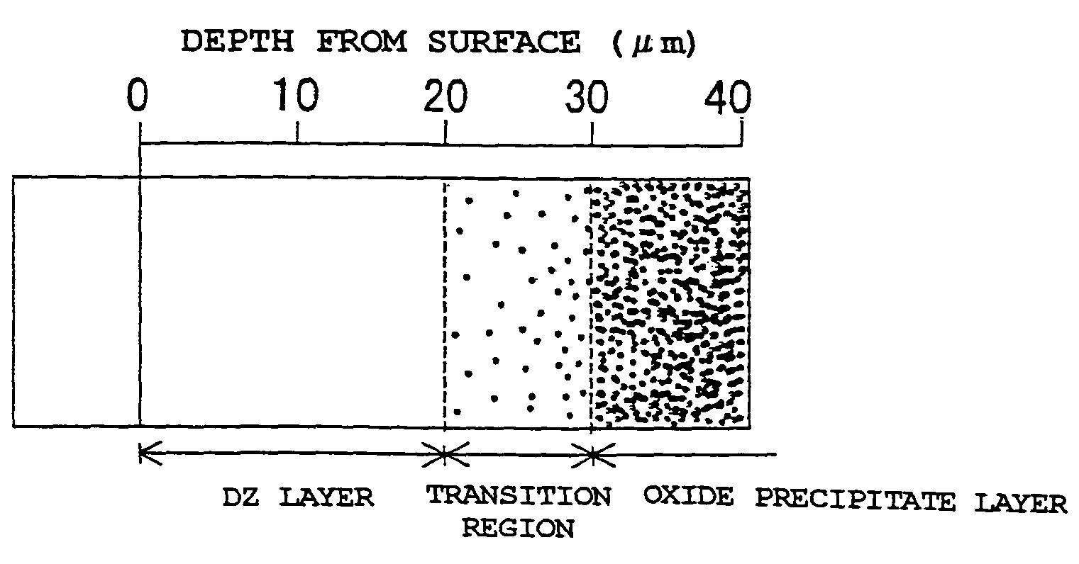
Image

Examples
experimental example 1
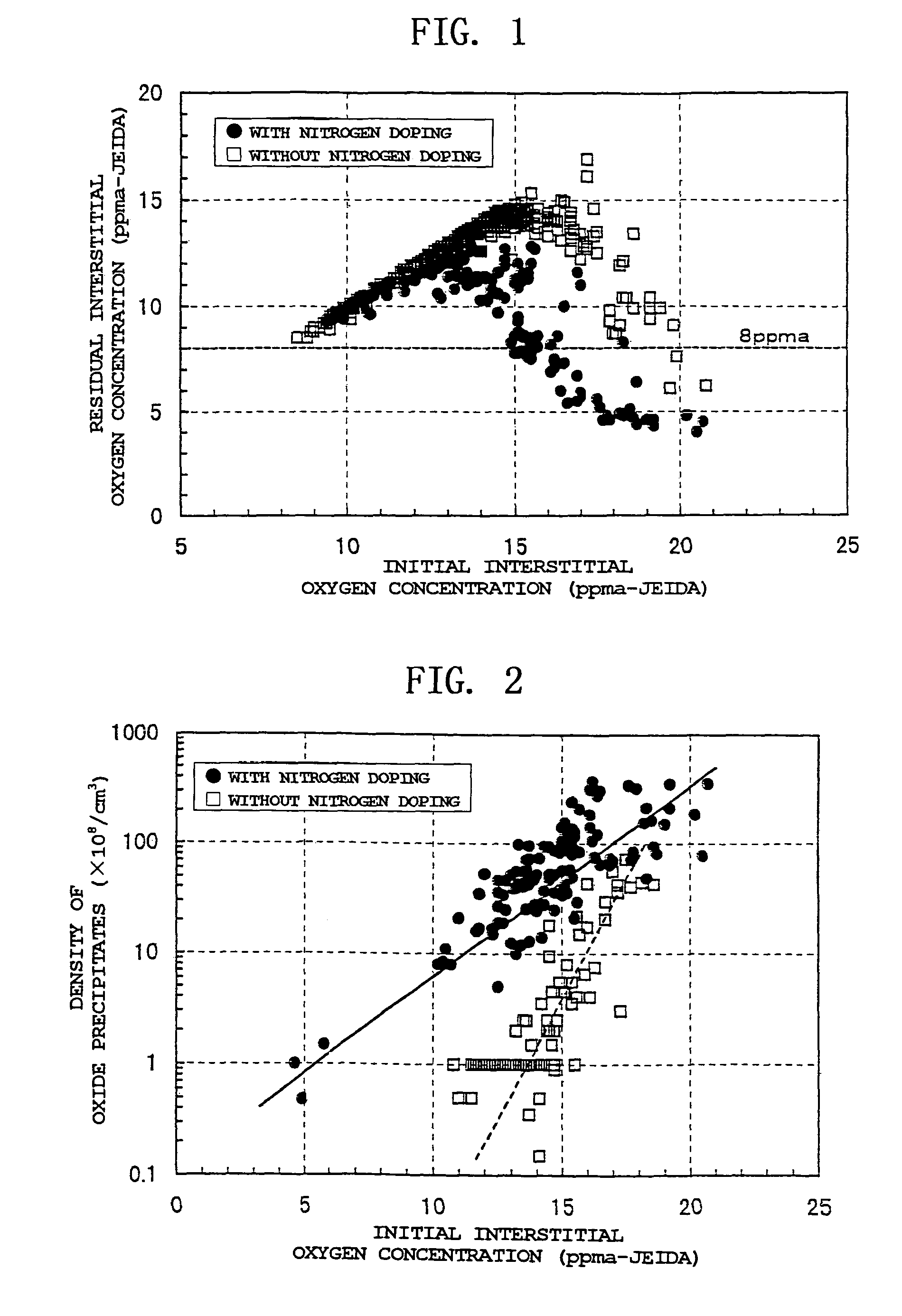
[0041]FIG. 1 shows experimental results representing relationship between the initial interstitial oxygen concentration and the residual interstitial oxygen concentration in various CZ wafers having an initial interstitial oxygen concentration of 8 to 21 ppma after they were subjected to usual heat treatments for oxygen precipitation, i.e., a heat treatment at 780° C. for 3 hours and a heat treatment at 1000° C. for 16 hours under a nitrogen atmosphere (containing 3% of oxygen). Two kinds of the nitrogen concentrations, i.e., 1×10¹³ to 9×10¹³ number / cm3 and no nitrogen doping, were used.
[0042]From the results shown in FIG. 1, it can be seen that if nitrogen is not doped, the residual interstitial oxygen concentration cannot be made 8 ppma or less after the aforementioned heat treatments unless the initial interstitial oxygen concentration is 19 ppma or more, whereas if nitrogen is doped, the range of acceptable initial interstitial oxygen concentration is enlarged to the range of 15...
experimental example 2
[0043]FIG. 2 shows experimental results representing relationship between the initial interstitial oxygen concentration and the density of precipitates in various CZ wafers having an initial interstitial oxygen concentration of 4 to 19 ppma after they are subjected to usual heat treatments for oxygen precipitation, i.e., a heat treatment at 780° C. for 3 hours and a heat treatment at 1000° C. for 16 hours under a nitrogen atmosphere (containing 3% of oxygen), angle polishing and preferential etching, in which the measured density of precipitates in the oxygen precipitation region was converted into volume density. Two kinds of the nitrogen concentrations, i.e., 1×10¹³ to 9×10¹³ number / cm3 and no nitrogen doping, were used.
[0044]From the results shown in FIG. 2, it can be seen that the oxide precipitate density is markedly increased by the nitrogen doping, even if the initial interstitial oxygen concentration is the same. It can be seen that, in particular, even with a low initial in...
example 1
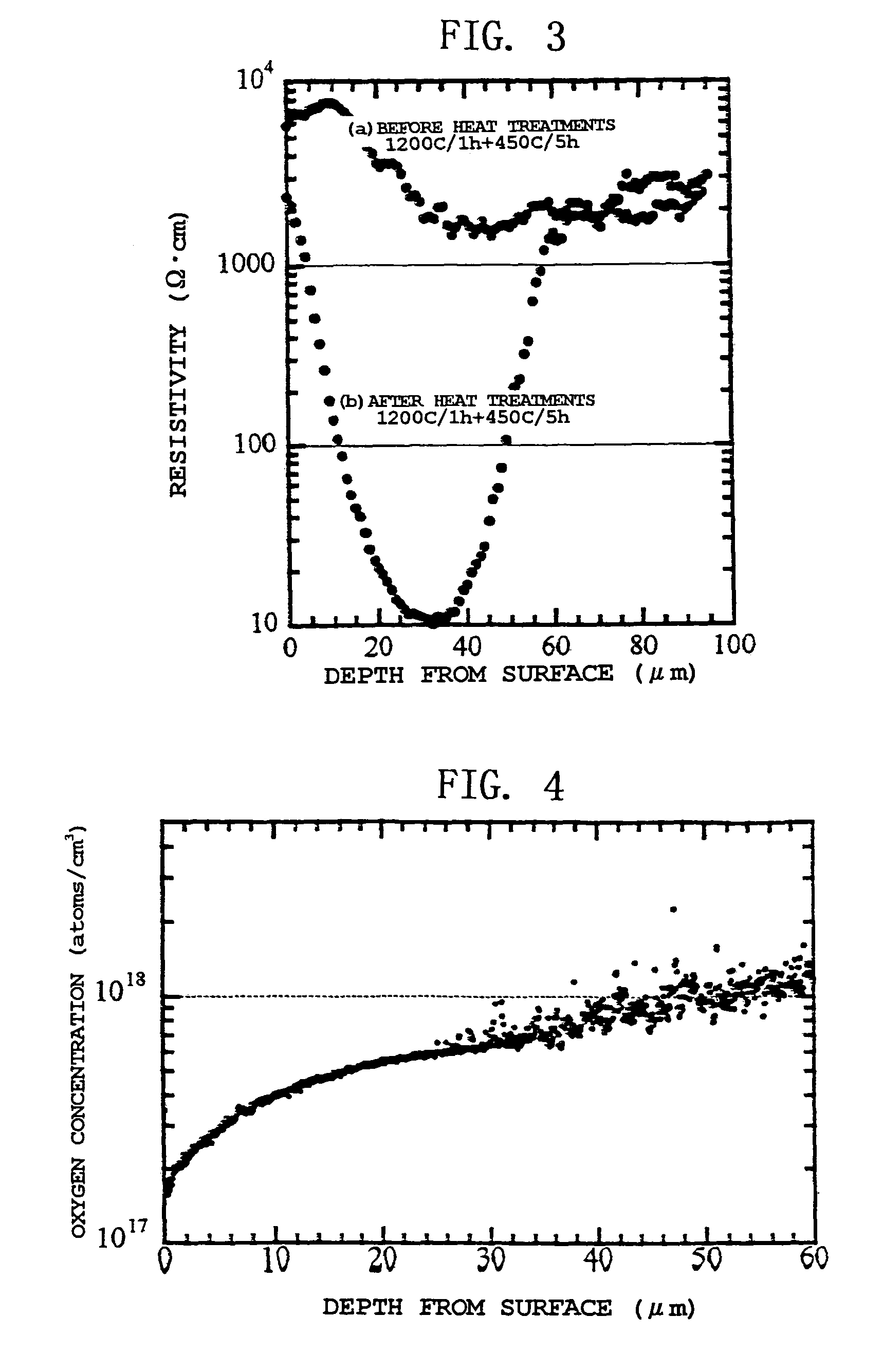
[0059]Silicon wafers having nitride films were introduced into raw material polycrystal, and a nitrogen-doped silicon single crystal was pulled by the CZ method (without applying magnetic field). The silicon single crystal was processed by a usual method to produce a CZ silicon wafer having a diameter of 200 mm, an initial interstitial concentration of 18 ppma (JEIDA), a nitrogen concentration of 8×10¹³ number / cm3 (calculated value) and a resistivity of 2500 Ω·cm.
[0060]This wafer was subjected to a heat treatment at 1100° C. for 2 hours and a heat treatment at 1000° C. for 16 hours under a 100% argon atmosphere and further subjected to heat treatments simulating a device production process (heat treatments at 1200° C. for 1 hour and at 450° C. for 5 hours) under a nitrogen atmosphere (mixed with 3% of oxygen) in a vertical type heat treatment furnace. For the silicon wafer obtained as described above, the residual interstitial oxygen concentration was measured by infrared absorption...
PUM
 Abstract
Description
Claims
Application Information