Doped nanoparticle-based semiconductor junction

a semiconductor junction and nanoparticle technology, applied in the field of doped semiconductor junctions, can solve the problems of insufficient device performance for market needs, relatively high cost, and limited efficiency, and achieve the effects of low cost, low cost, and low cos

Inactive Publication Date: 2009-10-20
NANOCO TECH LTD
View PDF7 Cites 13 Cited by
  • Summary
  • Abstract
  • Description
  • Claims
  • Application Information

AI Technical Summary

Benefits of technology

[0022]It is an advantage of the present invention to enable a simple method of forming doped semiconductor junctions comprised of nanoparticles. The semiconductor nanoparticles are doped either by in-situ or ex-situ processes. For the in-situ doping procedure, dopant materials are added during the process of synthetic growth of the colloidal nanoparticles. For the ex-situ doping procedure, a device layer is formed by coating on a surface a mixture of semiconductor and dopant material nanoparticles, wherein an anneal is performed to fuse the semiconductor nanoparticles and to enable dopant material atoms to diffuse out from the dopant material nanoparticles and into the fused semiconductor nanoparticle network. Semiconductor junctions composed of inorganic nanoparticles are typically highly resistive, which limits the usefulness of devices incorporating these junctions despite their low cost. By forming doped semiconductor junctions incorporating either in-situ or ex-situ doped inorganic nanoparticles, one can produce semiconductor junction devices at low cost while still maintaining good device performance. Doped semiconductor junctions help device performance by increasing the separation of the n- and p-Fermi levels, reducing ohmic heating, and aiding in forming ohmic contacts. By forming the doped semiconductor junction from inorganic nanoparticles, the device layers can be deposited by low cost processes, such as, drop casting, spin coating, or inkjetting. The resulting nanoparticle-based device can also be formed on a range of substrates, including flexible ones.
to enable a simple method of forming doped semiconductor junctions comprised of nanoparticles. The semiconductor nanoparticles are doped either by in-situ or ex-situ processes. For the in-situ doping procedure, dopant materials are added during the process of synthetic growth of the colloidal nanoparticles. For the ex-situ doping procedure, a device layer is formed by coating on a surface a mixture of semiconductor and dopant material nanoparticles, wherein an anneal is performed to fuse the semiconductor nanoparticles and to enable dopant material atoms to diffuse out from the dopant material nanoparticles and into the fused semiconductor nanoparticle network. Semiconductor junctions composed of inorganic nanoparticles are typically highly resistive, which limits the usefulness of devices incorporating these junctions despite their low cost. By forming doped semiconductor junctions incorporating either in-situ or ex-situ doped inorganic nanoparticles, one can produce semiconductor junction devices at low cost while still maintaining good device performance. Doped semiconductor junctions help device performance by increasing the separation of the n- and p-Fermi levels, reducing ohmic heating, and aiding in forming ohmic contacts. By forming the doped semiconductor junction from inorganic nanoparticles, the device layers can be deposited by low cost processes, such as, drop casting, spin coating, or inkjetting. The resulting nanoparticle-based device can also be formed on a range of substrates, including flexible ones.

Problems solved by technology

Most semiconductor devices in use today, both inorganic and organic, are in part or completely formed using expensive vacuum deposition processes.
There are ongoing efforts to find a low cost manufacturing process, but to date, device performance has been inadequate for market needs.
While these devices are useful in certain applications, their efficiency has been somewhat limited, yielding conversion efficiencies, e.g., solar power to electrical power, of typically marginally better than 10-20%.
Although efficiencies of these devices have been improving through costly improvements to device structure, the relative inefficiency of these devices, combined with their relatively high cost, have combined to inhibit the widespread adoption of solar electricity in the consumer markets.
However, the performance of these devices were not reported, and the conductivity of such a mixed photoactive layer is expected to be low due to the high resistivity of the polymeric binder.
A large part of the low efficiency was undoubtedly caused by the films being insulators (even after sintering) due to the lack of doping.
In addition, the process is inefficient with respect to usage of its starting materials.
However, either the resulting photovoltaic performance was sub-par or the deposition process had major drawbacks.
As a result of surface plasmon effects (K. B. Kahen, Appl. Phys. Lett. 78, 1649 (2001)), having metal layers adjacent to emitter layers results in a loss of emitter efficiency.
As is well known in the art, highly doping wide bandgap semiconductors is difficult as a result of self-compensation effects.
Consequently, forming ohmic contacts to these layers can prove to be difficult.
The dominant ones are high manufacturing costs, difficulty in producing multi-color output from the same chip, and the need for high cost and rigid substrates.
However, many of these dopants are unstable and the resistivities are many orders of magnitude higher than crystalline LED values of ˜0.1 ohm-cm.
The result of employing resistive layers is that one suffers from ohmic heating effects; it is difficult to make ohmic contacts; and since the drive current of the device is limited, so is the overall brightness of the device.
The above examples illustrate that higher performance semiconductor devices can be created from crystalline semiconductor materials; but with the drawback of high manufacturing costs.
Attempts to reduce the manufacturing costs by employing organic materials result in lower performance devices whose specifications sometimes fall significantly short of market requirements (e.g., organic-based photovoltaics).
Two approaches to lower the cost of crystalline semiconductor materials are to employ either amorphous or polycrystalline inorganic semiconductor materials; however, both of these approaches have well-known drawbacks.
Taking the case of devices formed from amorphous Si, both thin-film transistor and photovoltaic (PV) devices have significantly reduced performance due to low mobilities (and the Staebler-Wronski effect for PVs).
However, sputtering is a higher cost, vacuum-based deposition process and CBD, though chemically based, has long deposition times and is inefficient in its usage of starting materials, as stated previously.

Method used


Image

  • Doped nanoparticle-based semiconductor junction
  • Doped nanoparticle-based semiconductor junction
  • Doped nanoparticle-based semiconductor junction

Examples


example 1

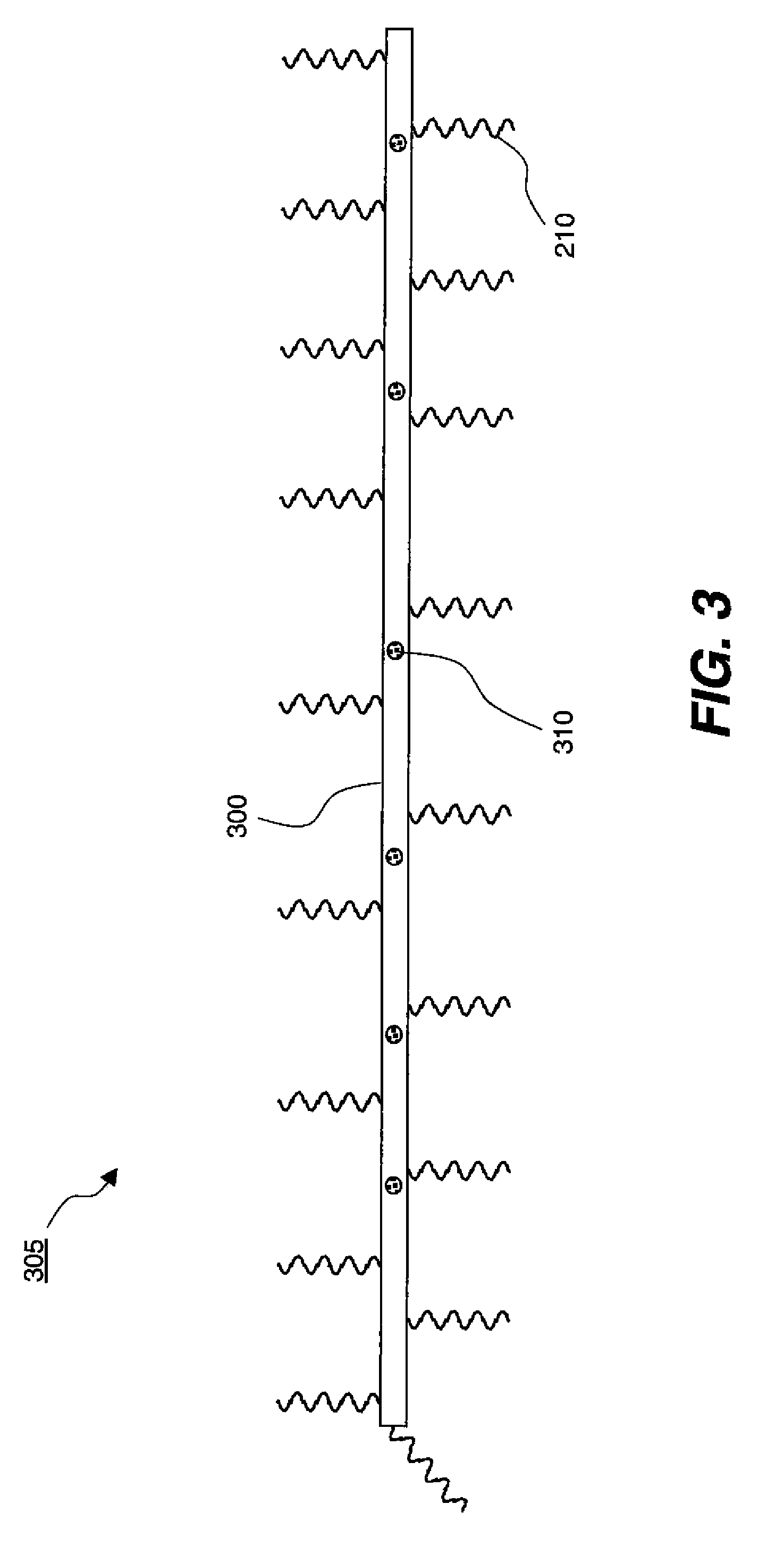
[0053]In this example the doped semiconductor junction 500 was formed between a p-Si substrate and an n-CdSe layer in-situ doped with In. The p-Si substrate had a resistivity of ˜5 ohm-cm. Doped CdSe quantum wires 300 were formed by a procedure based on that by Pradhan et al. (N. Pradhan et al., Nano Letters 6, 720 (2006)) for forming undoped CdSe nanowires. In our version the cadmium precursor is cadmium acetate, the indium precursor is indium acetate hydrate, and the Se precursor is selenourea. In the synthesis equal molar (1.27×10⁻⁴ moles) amounts are used of the cadmium acetate and the selenourea. Experimentation revealed that the resistivity of the doped CdSe layer was lowest when the In molar concentration was 0.1% of the cadmium molar concentration. The coordinating solvent for the growth was octylamine (OA), which was degassed at 30° C. for 30 minutes prior to its usage.

[0054]To form the cadmium precursor, in a small vial inside of a dry box, 0.03 g of cadmium acetate was ad...

example 2

[0060]In this example the doped semiconductor junction 500 was formed between a p-ZnTe layer ex-situ doped with Cu and an n-Si substrate. The n-Si substrate had a resistivity of ˜5 ohm-cm. Undoped ZnTe semiconductor nanoparticles 410 were synthesized by adapting the procedures commonly used to form ZnSe spherical dots (M. A. Hines et al., J. Phys. Chem. B102, 3655 (1998)). More specifically, 4 g of dried and degassed hexadecylamine (HDA) was placed in a three-neck flask and heated, under argon, to 290° C. on a Schlenk line. For the Te precursor, a 0.25 M solution (called TOPTe) of Te in trioctylphosphine (TOP) was formed by heating under vacuum a mixture of Te powder and TOP at 190° C., while vigorously stirring for ˜3-4 hours. The resulting solution was clear and had a green-yellow appearance. In a dry box, a syringe was filled with 0.4 mmol of diethylzinc (from a 1 M diethylzinc in hexane solution), 1.6 mmol of TOPTe, and 2.0 ml of additional TOP. The syringe contents were quickly...

example 3

[0069]In the final example the doped semiconductor junction 500 was formed between a p-ZnTe layer ex-situ doped with Cu and an n-CdSe layer in-situ doped with In. For ease of contacting the n-CdSe, it was deposited on n-Si, instead of glass. Thus, the total diode structure was p-ZnTe:n-CdSe:n-Si. Both the Cu-doped ZnTe layer and the In-doped CdSe layer were formed using the same dispersions employed for Examples 2 and 1, respectively. Starting with 19 mm square n-Si pieces, analogous procedures (see Examples 1 and 2) were followed for applying Al metal to the n-Si backside and drop casting both nanoparticle-based dispersions. All of the drop castings were performed in a dry box in order to prevent oxide formation on the semiconductor surfaces. Prior to drop casting the mixed Cu and ZnTe dispersion on the n-CdSe film surface, the film surface was washed with acetone and methanol. After the In-doped n-CdSe film deposition, the diode was annealed as described in Example 1; after the Cu...


PUM


Abstract

A doped semiconductor junction for use in an electronic device and a method for making such junction is disclosed. The junction includes a first polycrystalline semiconductor layer doped with donors or acceptors over a substrate such that the first doped semiconductor layer has a first polarity, the first layer including fused semiconductor nanoparticles; and a second layer in contact with the first semiconductor layer over a substrate to form the semiconductor junction.

Description

[0001]This invention was made with Government support under Cooperative Agreement #DE-FC26-06NT42864 awarded by DOE. The Government has certain rights in this invention.CROSS-REFERENCE TO RELATED APPLICATIONS[0002]Reference is made to commonly assigned U.S. patent application Ser. No. 11 / 668,041 filed Jan. 29, 2007, entitled “Doped Nanoparticle Semiconductor Charge Transport Layer” by Keith B. Kahen, and U.S. patent application Ser. No. 11 / 677,794 filed Feb. 23, 2007, entitled “Ex-Situ Doped Semiconductor Transport Layer” by Keith B. Kahen, the disclosures of which are incorporated herein.FIELD OF THE INVENTION[0003]The present invention relates to doped semiconductor junctions containing nanoparticles and a method for making such junctions.BACKGROUND OF THE INVENTION[0004]A variety of semiconductor devices, such as, bipolar transistors, rectifying diodes, light emitting diodes (LEDs), lasers, photodetectors, solar cells and others, require the formation of doped semiconductor junct...

Claims


Application Information

Patent Timeline
Patent Type & Authority Patents(United States)
IPC IPC(8): H01L21/20
CPCB82Y10/00H01L21/02381H01L21/02524H01L21/02538H01L21/02551H01L21/0256H01L21/02562H01L21/02568H01L21/02576H01L21/02579H01L21/02581H01L21/02601H01L21/02628H01L29/0665H01L29/0673H01L29/861H01L29/868B82Y30/00H01L33/18Y10S977/892
Inventor KAHEN, KEITH B.
Owner NANOCO TECH LTD
Why Eureka
Try Eureka