Single transistor charge transfer random access memory

Inactive Publication Date: 2011-07-05
DALTON DAVID I +1
View PDF13 Cites 4 Cited by
  • Summary
  • Abstract
  • Description
  • Claims
  • Application Information

AI Technical Summary

Benefits of technology

[0005]Disclosed herein is a memory device, a memory cell and method for producing the same which preserves the advantages of a flash device (prior art) such as nonvolatility, small c

Problems solved by technology

Such memories are known to exhibit excellent retention characteristics, but have margina

Method used


Image

  • Single transistor charge transfer random access memory
  • Single transistor charge transfer random access memory
  • Single transistor charge transfer random access memory

Examples


Embodiment Construction

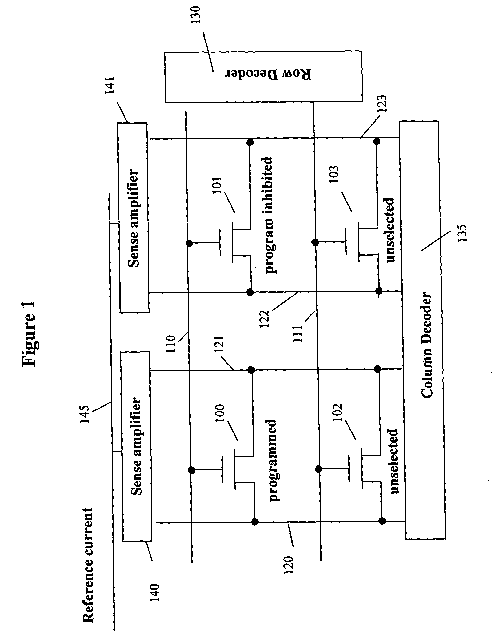
[0025]FIG. 1 is a schematic representation of a 2×2 array of single transistor memory cells arranged in rows and columns according to one embodiment of the present invention. The gate electrodes of the transistors in a common row are connected to and share a common word line. For example, devices 100 and 101 share word line 110, and devices 102 and 103 share word line 111. The sources and drains of the transistors in a common column share a common bit line pair. For example, the sources of transistors 100 and 102 share bit line 120, while drains share a common (complement) bit line 121. The sources of transistors 101 and 103 share bit line 122, while drains share a common (complement) bit line 123. In another embodiment of the invention bit line 121 and complement bit line 122 are combined and form a common bit line. A given word line is selected by a row decoder 130. One or more bit line pairs are selected by column decoder 135. A sense amplifier is connected to each bit line pair ...


PUM


Abstract

A nonvolatile semiconductor memory device is described where each memory cell is composed of a single field effect transistor with a dual gate dielectric comprising a dielectric interfacial layer in contact with a silicon substrate and a ferroelectric layer in between the interfacial layer and the gate electrode. To program (write) the cell the ferroelectric layer is polarized in one of two directions, the ferroelectric polarization creating a large electric field in the interfacial layer. This electric field causes electrons or holes to be transported across the interfacial layer and be trapped in the ferroelectric layer establishing a high (erased) or low (programmed) threshold voltage depending on the direction of the ferroelectric polarization representing the two logic states. To read the memory cell a voltage is applied to the drain of the selected transistor and depending on whether a high or low threshold state was programmed into the cell a low or high current is sensed.

Description

RELATED APPLICATION[0001]The present application is related to and claims priority from U.S. Provisional Application Ser. No. 60 / 599,712, filed Aug. 6, 2004, entitled “FERROELECTRIC TUNNEL RANDOM ACCESS MEMORY”. The disclosure of the provisional application is herein specifically incorporated in its entirety by this reference.STATEMENT REGARDING FEDERALLY SPONSORED RESEARCH OR DEVELOPMENT[0002]This invention was made with Government support under contract DASG60-01-C-0046 awarded by the U.S. Army Space and Missile Defense Command. The Government has certain rights to this invention.FIELD OF THE INVENTION[0003]The invention disclosed relates to the field of nonvolatile semiconductor memory devices and more particularly to memory devices using a single transistor in the memory cell with a dual layer gate dielectric composed of a dielectric interfacial layer and a ferroelectric layer.BACKGROUND OF THE INVENTION[0004]Nonvolatile semiconductor memory devices represent a multibillion-doll...

Claims


Application Information

Patent Timeline
IPC IPC(8): H01L29/76
CPCG11C11/22H01L29/78391H01L29/516H01L21/28291G11C11/223H01L29/40111
Inventor DALTON, DAVID I.GNADINGER, ALFRED P.
Owner DALTON DAVID I
Why Eureka
Try Eureka