High-temperature, wirebondless, injection-molded, ultra-compact hybrid power module

a hybrid power module and high-temperature technology, applied in the field of high-power and high-temperature hybrid power module packaging, can solve the problems of shortening the power handling capability and other requirements, unable to meet the requirements of high-temperature packaging systems, and the package is limited to relatively low current applications, so as to achieve cost-effective effects

Active Publication Date: 2012-02-21
UNIV OF CENT FLORIDA RES FOUND INC
View PDF26 Cites 27 Cited by
  • Summary
  • Abstract
  • Description
  • Claims
  • Application Information

AI Technical Summary

Benefits of technology

[0026]It is a primary objective of the present invention to provide a cost-effective, ultra-compact, hybrid power module packaging technology that allows devices to operate at over 300° C.

Problems solved by technology

However, a major limitation to fully realizing the potential of SiC and other wide band-gap semiconductor materials is the lack of qualified high-temperature packaging systems, particularly those with high-current and high-voltage capabilities required for power conversion applications.
The commercial SiC Schottky diodes currently available are only rated for an operating junction temperature up to 175° C. due to the limitation of the conventional plastic packages used.
The high-reliability packaging schemes used today for military applications do offer considerable high temperature operation capability, but fall short on power handling capability and other requirements.
However, these packages are limited to relatively low current applications due to the use of thin Au wires (typically 2-5 mils in diameter).
Paralleling these packages for higher current capability may be feasible for low-frequency power converters, but does not provide a viable solution for high-density high-performance power electronic systems due to the inevitable large parasitic impedance and physical dimensions associated.
Temperature limitations for ceramic packages depend on the type of sealing method used.
However, ceramic packages are not suitable for high-current applications due to the high resistance of the refractory metal interconnects used inside the packages.
However, today's plastic packages are not suitable for operating temperature above 150° C. For example, the glass transition temperature of commonly used packaging epoxies is in the range of 130-170° C., which limits the operating temperature range of the package.
Plastic packages also subject wire bonds to extreme stresses if the package undergoes large temperature swings.
The thin aluminum wirebonds suffer from high parasitic impedance, fatigue-induced lift-off failures, and inability of removing heat.
The DBC ceramic substrate, aluminum oxide (Al2O3) or more expensive aluminum nitride (AlN), provides electrical isolation but inadvertently increases the package thermal resistance.
The easy oxidation of Cu, low melting temperatures of the tin / lead (Sn / Pb) solder joints of chip-to-DBC and DBC-to-baseplate, and low glass transition temperature of the epoxy case all prevent the use of the conventional power modules in high temperature applications.
However, this approach does not offer high current handling capability due to the high resistance of the thick-film Au or Pt interconnection layer used.
Problems still exists with the prior art described above.
Many factors have to be considered in the preparation of satisfactory high-temperature electronic packaging, so the devices are often very complicated and costly.
None of the prior art references is entirely without technical merits, those aluminum nitride (AlN)-based high temperature modules are essentially very costly duplicates of the existing conventional temperature hybrid module technology, which is, unfortunately, a 20-year old technology due for an overhaul itself.
The biggest problem of a conventional power module is the complexity of its material system, which is comprised of multiple semiconductor chips, one or more ceramic substrates with patterned metal interconnect films, a metal baseplate, Al or Au wirebonds connecting the semiconductor chips to the substrate metal layer, soldering joints of semiconductor-to-substrate and substrate-to-baseplate, epoxy sidewall module case, external metal posts or feedthroughs, and silicon-gel potting material.
Such a module construction method unnecessarily increases the module's weight, size, and junction-to-case thermal resistance.
More critically, the complex material system creates many joints and interfaces between dissimilar materials, which tend to cause reliability concerns at high temperatures or under thermal cycling conditions.
For example, it is well known that aluminum wirebonds tend to fail by creep deformation at high temperatures, and tin / lead (Sn / Pb) solder joints suffer from voids or delineation under thermal cycling in the conventional power modules.
In short, the existing hybrid power module technology, limited by its material and construction complexity, does not provide a good platform for new high temperature module development.
It is simply not enough just to substitute the materials in the conventional module architecture with newer and more costly high-temperature alternatives.
More disruptive technological innovation in both module architecture and material selection is needed to provide smaller, lighter, cheaper, and more reliable modules for high temperature power electronics in both military and commercial applications.

Method used


Image

  • High-temperature, wirebondless, injection-molded, ultra-compact hybrid power module
  • High-temperature, wirebondless, injection-molded, ultra-compact hybrid power module
  • High-temperature, wirebondless, injection-molded, ultra-compact hybrid power module

Examples


first embodiment

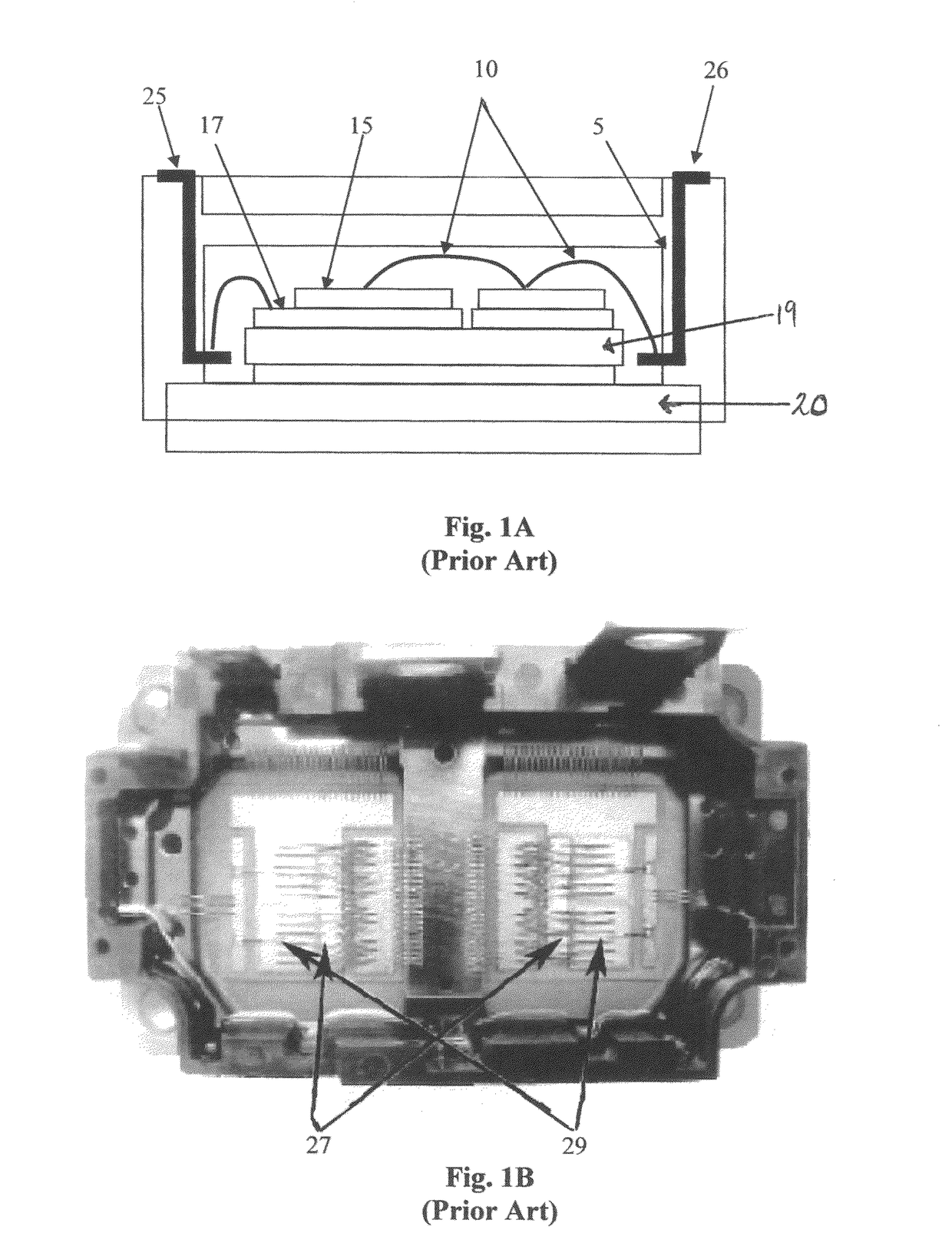
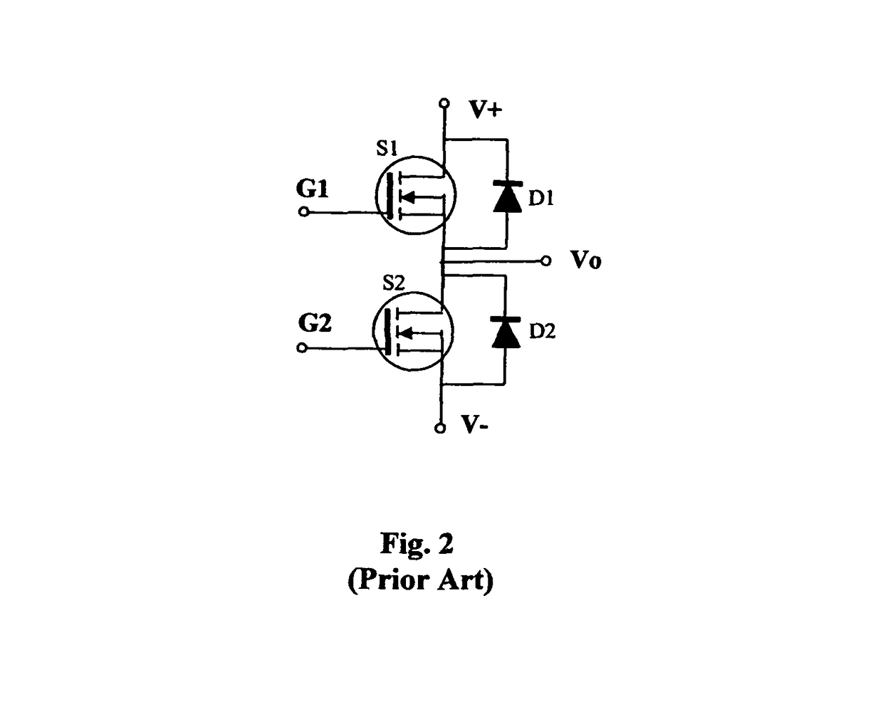
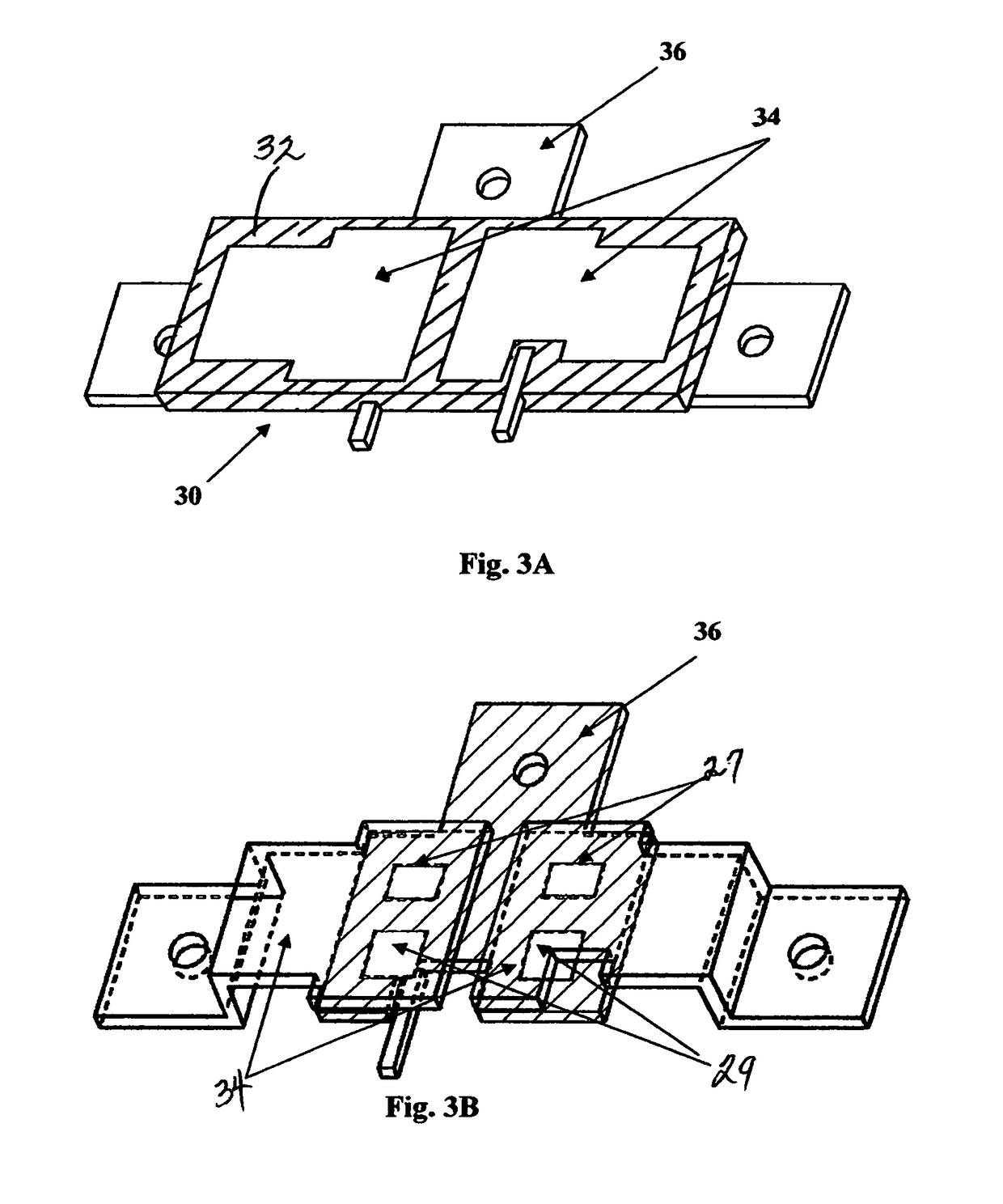
[0058]A novel hybrid power module concept is disclosed based on the use of double metal leadframes, direct leadframe-to-chip bonding, and injection-molded high temperature polymer encapsulation. A half-bridge circuit, consisting of two active SiC switches and two anti-parallel SiC Schottky diodes, is used for the purpose of illustration and specification of the prototype module design. The half-bridge circuit commonly used in conventional power modules is shown in FIG. 2. In FIG. 2, S1 and S2 are SiC power MOSFETs while D1 and D2 are SiC Schottky diodes.

[0059]The power module in FIG. 2 is the most basic building block in power electronics, which can be used in various combinations in electric vehicle motor drive inverters, power supply DC / DC converters, uninterruptible power supply DC / AC inverters, and many other applications. Nevertheless, the module construction of the present invention can be easily adapted to other circuit configuration such as 3-phase inverters or even RF power...

second embodiment

[0074]This embodiment is intended for medium or conventional temperature applications. The basic module structure remains the same as shown in FIGS. 6A and 6B. However, the leadframes can be made of copper (Cu) or Cu alloys instead of Mo. Silicon (Si) or silicon carbide (SiC) semiconductor chips 60 can be soldered to the leadframes using conventional soft solders such as tin / lead (Sn / Pb) solder paste. Conventional plastic encapsulation materials can be used as the molding compound to form the module encapsulation 70. When compared to the prior art conventional temperature power module, the new module still maintains most of the advantages described herein.

[0075]FIG. 7A provides a smaller configuration 80 of the hybrid power module of the present invention wherein a single SiC chip is used. FIG. 7B is an exploded view of the single chip diode power module 80 with a sandwich arrangement of a top metal leadframe 84 and a bottom metal leadframe 86 with the SiC chip 82 between the two le...


PUM

PropertyMeasurementUnit
thicknessaaaaaaaaaa
thicknessaaaaaaaaaa
thicknessaaaaaaaaaa

Abstract

A cost-effective, ultra-compact, hybrid power module packaging system and method for making allows device operation in conventional and high temperature ranges over 300° C. Double metal leadframes are directly bonded to the front- and backside of semiconductor chips, and injection-molded high temperature polymer materials encapsulate the module. The invention eliminates the use of unreliable metal wirebonds and solders joints, and expensive aluminum nitride ceramic substrates commonly used in conventional and high temperature hybrid power modules. Advantages of the new power modules include high current carrying capability, low package parasitic impedance, low thermo-mechanical stress under high temperature cycling, low package thermal resistance (double-side cooling), modularity for easy system-level integration, and low-cost manufacturing of devices compatible with current electronic packaging industry. A first embodiment uses molybdenum leadframes for operation in temperatures over 300° C.; a second embodiment of the invention, uses copper and copper alloy leadframes, provides benefits for conventional temperature electronics.

Description

[0001]This application claims the benefit of priority from U.S. Provisional Patent Application 60 / 718,132, filed on Sep. 16, 2005.FIELD OF THE INVENTION[0002]This invention relates to electronic packaging technology and, in particular to, high-power and high-temperature hybrid power module packaging.BACKGROUND AND PRIOR ART[0003]Silicon carbide (SiC) is widely considered as the power semiconductor of choice due to its wide energy band-gap, high breakdown field strength, high operating junction temperature, high carrier saturation drift velocity, and high thermal conductivity. SiC devices offer great potential for use in high-temperature, high-power, high-frequency, and radiation-resistant military applications such as ultra-compact, ultra-light power conversion units for in-ground power sources, hybrid military vehicles, electric aircraft and ships, and nuclear power instrumentation.[0004]SiC devices can also be used in a wide range of commercial applications including hybrid electr...

Claims


Application Information

Patent Timeline
Patent Type & Authority Patents(United States)
IPC IPC(8): H01L23/495H01L23/29
CPCH01L21/565H01L23/49568H01L23/49861H01L23/49537H01L2924/3011H01L2224/48137H01L2224/48247H01L2924/09701H01L24/48H01L2924/01322H01L2924/01327H01L2924/13091H01L2924/13055H01L2924/15747H01L2224/45124H01L2224/45144H01L2924/12032H01L2924/30107H01L2924/00H01L2224/45015H01L2924/00014H01L24/45H01L2924/19107H01L2924/181H01L2224/48139H01L2924/00015H01L2224/05599
Inventor SHEN, ZHENG JOHN
Owner UNIV OF CENT FLORIDA RES FOUND INC
Why Eureka
Try Eureka