Germanium-painting structure for insulating layer of mixed graphical monocrystaline silicon as well as method and application thereof

A technology of germanium and single crystal silicon on the insulating layer, which is applied in the field of microelectronics, can solve the problems of large leakage current, small band gap, and difficulty in obtaining high-quality single crystal germanium compared with silicon, so as to reduce leakage current and improve work efficiency. Speed, the effect of promoting optoelectronic integration

Inactive Publication Date: 2008-12-17
SHANGHAI INST OF MICROSYSTEM & INFORMATION TECH CHINESE ACAD OF SCI +1
View PDF0 Cites 22 Cited by
  • Summary
  • Abstract
  • Description
  • Claims
  • Application Information

AI Technical Summary

Problems solved by technology

However, we also need to note that the content of germanium materials in the earth's crust is low, and it is more difficult to obtain high-quality single crystal germanium than silicon
Moreover, the band gap of Ge material is small (about 0.67eV at room temperature), which leads

Method used


Image

  • Germanium-painting structure for insulating layer of mixed graphical monocrystaline silicon as well as method and application thereof
  • Germanium-painting structure for insulating layer of mixed graphical monocrystaline silicon as well as method and application thereof
  • Germanium-painting structure for insulating layer of mixed graphical monocrystaline silicon as well as method and application thereof

Examples


Embodiment 1

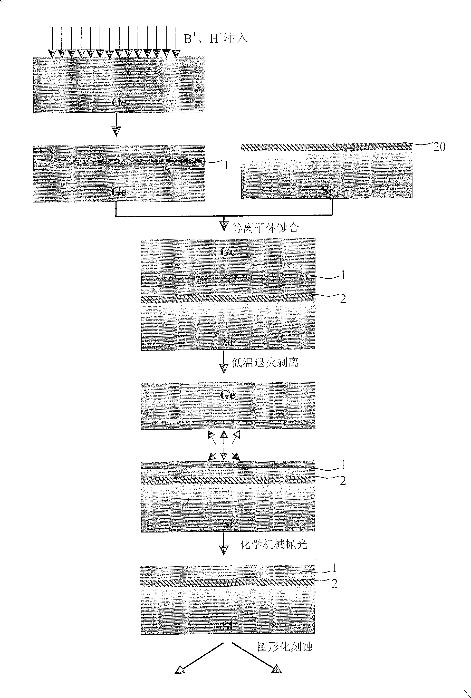
[0018] Embodiment 1: The preparation method of low-temperature GeOI structure film.

[0019] The steps are shown in Figure 1:

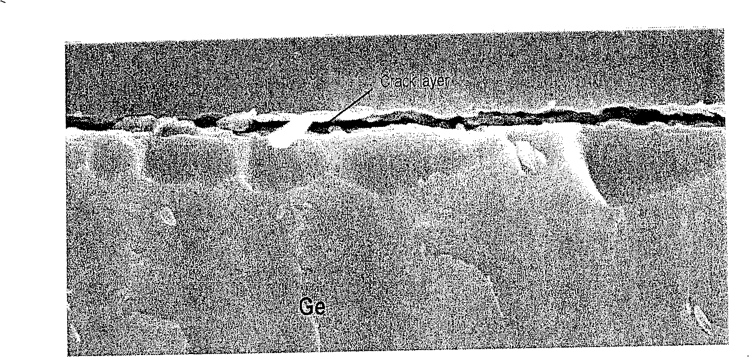
[0020] 1. Boron ion, hydrogen ion implantation: Firstly, the dose is implanted on the germanium wafer with a dose of 5×10 15 cm -2 of boron ions, and then implanted 5×10 16 cm -2 Hydrogen ions, 10 are defect layers caused by co-implantation of boron ions and hydrogen ions into germanium wafers.

[0021] 2. Plasma bonding: chemically clean the silicon wafer covered with silicon dioxide film and the germanium wafer implanted with perboron hydride ions to remove surface sticking dirt, and then activate the surface with low-temperature nitrogen plasma after drying. The nitrogen plasma activation conditions are: air pressure 0.4 mbar, plasma power 100W, high-purity nitrogen gas flow rate 80 sccm. After activation, rinse with deionized water for 6 seconds, rinse with megasonic water for 6 seconds and then spin dry, then bond the two pieces face to face...

Embodiment 2

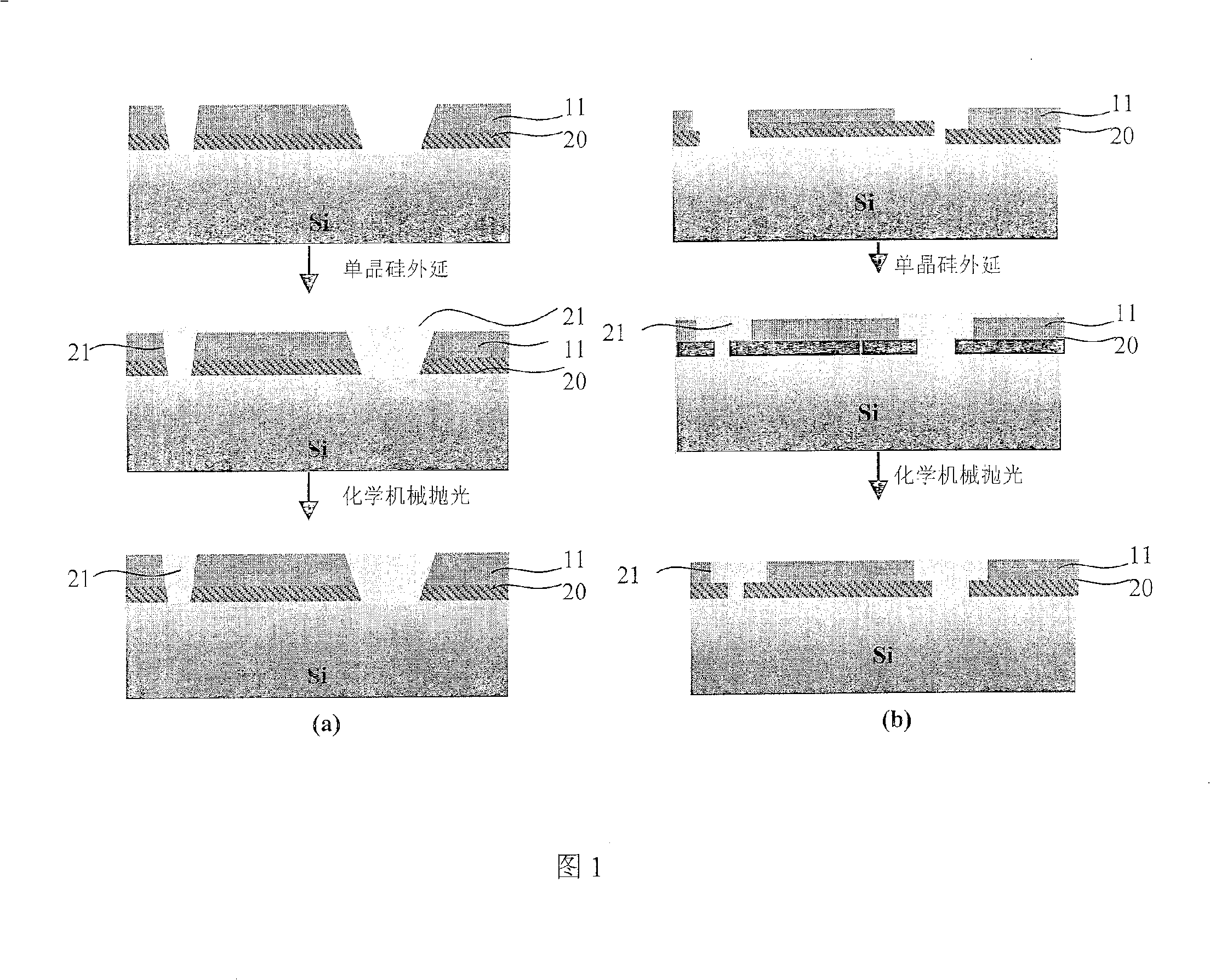
[0024]Embodiment 2: A method for preparing a GeOI structure of mixed patterned single crystal silicon.

[0025] 1. Pattern the germanium (GeOI) thin film on the insulating layer obtained in Example 1 according to the requirements, and use the same window mask to etch the top layer of germanium and the lower oxide layer. Reactive ion etching or wet etching is used to remove the top germanium layer and the underlying silicon dioxide insulating buried layer to expose the patterned bottom substrate (100) silicon.

[0026] 2. Use ultra-high vacuum chemical vapor deposition (UHVCVD) to perform epitaxy on the etched window to obtain a GeOI structure containing patterned silicon, in which the single crystal silicon is in the (100) crystal orientation.

[0027] 3. Use CMP to remove the excess epitaxial silicon and silicon dioxide protective layer on the top layer of germanium, and polish the surface, finally as shown in Figure 1(a).

Embodiment 3

[0028] Embodiment 3: GeOI structures of different insulating buried layers and preparation of silicon on patterned insulating layers with different crystal orientations.

[0029] 1. In embodiment 1, can select to deposit the substrate silicon chip of different insulating buried layers, as silicon nitride, aluminum nitride, a kind of of aluminum oxide or diamond-like carbon, or the compound structure that is formed by them to improve buried layer thermal conductivity. The crystal orientation of the substrate silicon wafer determines the crystal orientation of the epitaxial silicon, which can be (110) or (100). (100) substrates can be selected for electron-type working devices on patterned silicon, and (110) substrates can be selected for hole-type working devices.

[0030] 2. Similar to the method of embodiment 2, the germanium (GeOI) film on the insulating layer obtained in embodiment 1 is subjected to patterning photolithography according to requirements, and the window of e...


PUM

PropertyMeasurementUnit
Thicknessaaaaaaaaaa

Abstract

The invention relates to a germanium-on-insulator (GeOI) structure mixed with patterned single-crystal silicon and a manufacturing method thereof. The GeOI structure is characterized in that an active layer is composed of single-crystal germanium and single-crystal silicon, and the crystal orientation of the single-crystal silicon is determined by substrate silicon. The key point for preparing the structure is to prepare a GeOI single-crystal film. The substrate with the GeOI structure mixed with patterned single-crystal silicon is prepared by the steps of: transferring a single-crystal germanium film on an insulator by using plasma low temperature bonding and low temperature stripping techniques, and performing selective etching and single-crystal silicon epitaxy on the single-crystal germanium film. The inventive GeOI structure mixed with patterned single-crystal silicon can be used for gallium arsenide epitaxy, so as to integrate with III-V semiconductors. Meanwhile, the patterned single-crystal silicon material can be used for conventional CMOS processing to prepare conventional devices and circuits, so as to effectively solve the self healing effect of an embedded oxidation layer. The GeOI structure mixed with patterned single-crystal silicon has important application prospects in high-speed high-performance CMOS devices, optoelectronic integrated circuits, high-speed photodetectors, etc.

Description

technical field [0001] The invention relates to a germanium structure on an insulating layer of mixed patterned single crystal silicon and a manufacturing method thereof, belonging to the field of microelectronics. Background technique [0002] With the development of large-scale integrated circuit manufacturing technology, the feature size of its devices is also shrinking. Since 2006, the 65nm production lines of Intel Corporation, Texas Instruments, South Korea's Samsung, and Japan's Toshiba have successively entered the mass production stage, and 32nm and 22nm CMOS technologies are in the research and development stage. The development of integrated circuits has reached the current extremely large-scale era, and the existing bulk silicon materials and processes are approaching their physical limits. To further improve circuit speed and device performance, new breakthroughs must be made in materials and processes in order to achieve CMOS in the future. Moore's Law is main...

Claims


Application Information

Patent Timeline
IPC IPC(8): H01L21/18
Inventor 马小波刘卫丽宋志棠李炜林成鲁
Owner SHANGHAI INST OF MICROSYSTEM & INFORMATION TECH CHINESE ACAD OF SCI
Why Eureka
Try Eureka