Double-channel MOS-HEMT (Metal Oxide Semiconductor-High Electron Mobility Transistor) device and manufacturing method

A dual-channel, device technology, used in semiconductor/solid-state device manufacturing, semiconductor devices, electrical components, etc., can solve the problems of obvious self-heating effect, serious gate leakage current, current collapse effect, etc., to reduce the self-heating effect. , The effect of reducing gate leakage current and high breakdown voltage

Inactive Publication Date: 2010-12-15
SHANGHAI INST OF TECHNICAL PHYSICS - CHINESE ACAD OF SCI
View PDF5 Cites 27 Cited by
  • Summary
  • Abstract
  • Description
  • Claims
  • Application Information

AI Technical Summary

Problems solved by technology

However, AlGaN/GaN/AlGaN/GaN dual-channel HEMTs also have obvious disadvantages: 1. The self-heating effect is obvious; 2. The curr

Method used


Image

  • Double-channel MOS-HEMT (Metal Oxide Semiconductor-High Electron Mobility Transistor) device and manufacturing method
  • Double-channel MOS-HEMT (Metal Oxide Semiconductor-High Electron Mobility Transistor) device and manufacturing method
  • Double-channel MOS-HEMT (Metal Oxide Semiconductor-High Electron Mobility Transistor) device and manufacturing method

Examples


Example Embodiment

[0050] Example

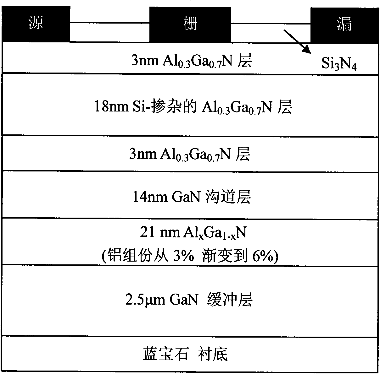
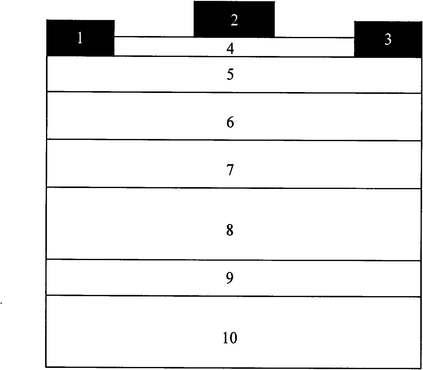
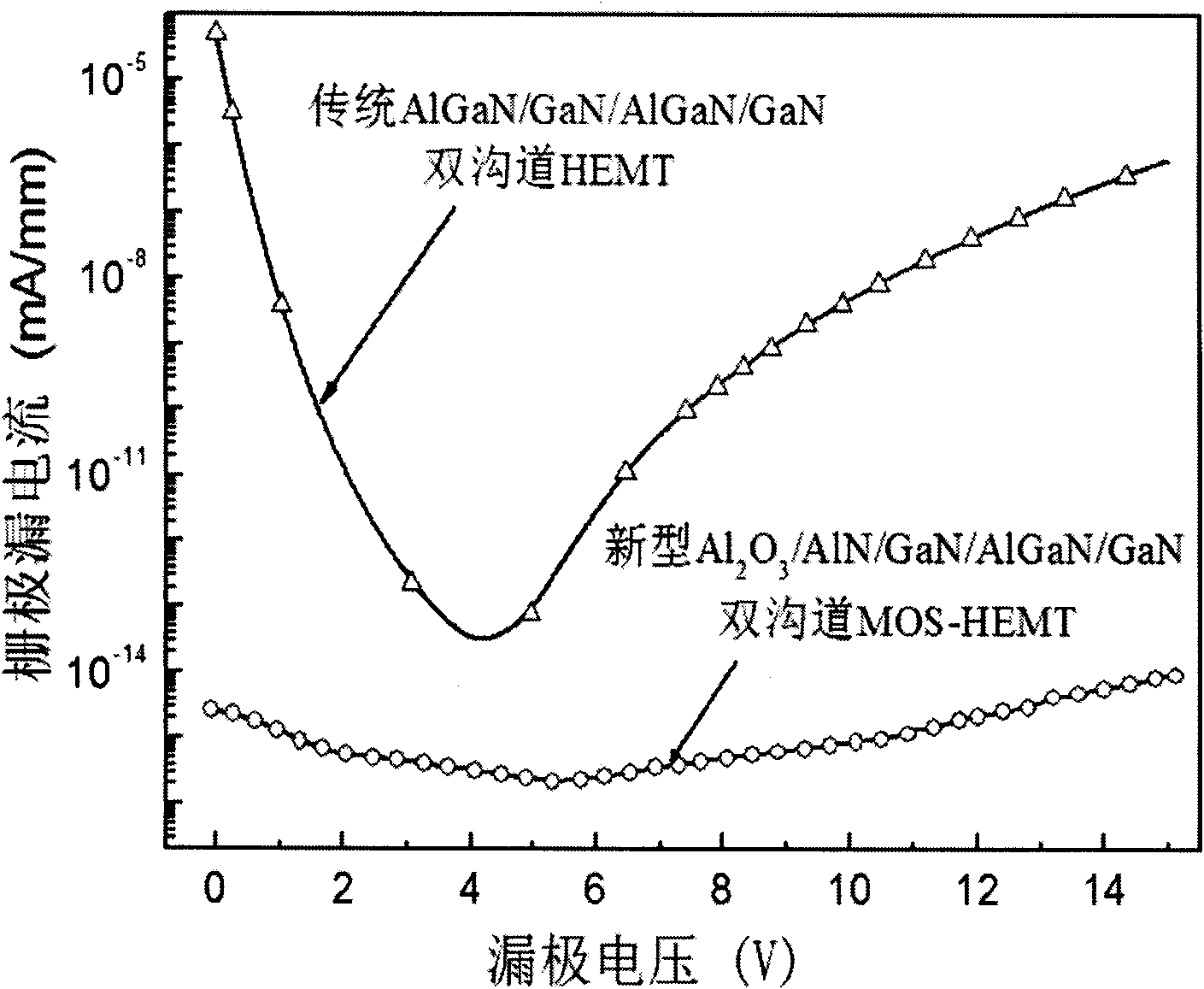
[0051] The present invention simulates the traditional AlGaN / GaN / AlGaN / GaN dual-channel HEMT and the Al 2 o 3 The electrical characteristics of the / AlN / GaN / AlGaN / GaN dual-channel MOS-HEMT thus prove the superiority of the new device of the present invention in suppressing current collapse and self-heating effects compared with traditional devices. image 3 To compare the relationship between the gate leakage current and the drain voltage of the device of the present invention and the traditional device, it can be seen from the figure that the gate leakage current of the device of the present invention is lower than that of the traditional device by more than 4 orders of magnitude. Figure 4 For the comparison of the output characteristics of the device of the present invention and the traditional device, it can be seen from the figure that the drain current density of the device of the present invention has obviously increased, which shows that the polariz...


PUM

PropertyMeasurementUnit
Thicknessaaaaaaaaaa
Thicknessaaaaaaaaaa

Abstract

The invention discloses an Al2O3/AlN/GaN/AlGaN/GaN double-channel MOS-HEMT (Metal Oxide Semiconductor-High Electron Mobility Transistor) device and a manufacturing method. The double-channel MOS-HEMT device comprises a GaN nucleating layer 9, a GaN buffer layer 8, an AlGaN lower barrier layer 7, a GaN channel layer 6, an AlN upper barrier layer 5, an Al2O3 gate dielectric layer 4, a source electrode 1, a drain electrode 3 and a gate electrode 2, wherein the GaN nucleating layer 9, the GaN buffer layer 8, the AlGaN lower barrier layer 7, the GaN channel layer 6 and the AlN upper barrier layer 5 are formed on a sapphire substrate 10 in sequence, the Al2O3 gate dielectric layer 4, the source electrode 1 and thea drain electrode 3 are formed on the AlN upper barrier layer 5, and the gate electrode 2 is formed on the Al2O3 gate dielectric layer 4. The invention is characterized in that an AlN material with good heat conductivity and greater forbidden band width is used as the upper barrier layer, so that the self heating effect of the device is reduced, and the threshold voltage of the device in a depletion mode is reduced; a depth potential well made from AlN and GaN is used for suppressing the hot electron effect under high voltage, so that the current collapse effect of the device is reduced; the strong polarization feature of the AlN material is used to increase the electron concentration in the channel and increase the saturation current and the output power of the device; and the Al2O3 material deposited by using the atomic layer deposition process is used as the gate dielectric layer, so that the leakage current of the gate electrode is reduced, and the breakdown voltage of the device is increased.

Description

technical field [0001] The present invention relates to electronic component technology, in particular to Al with a high concentration of two-dimensional electron gas 2 o 3 / AlN / GaN / AlGaN / GaN dual-channel MOS-HEMT devices, which can be used in high-temperature, high-frequency, high-power applications, high-power switches, and digital circuits. Background technique [0002] The third-generation wide-bandgap semiconductor devices represented by gallium nitride and silicon carbide are new types of wide-bandgap semiconductor devices that have developed rapidly in the past 10 years after the first and second-generation semiconductor devices (Si, GaAs). Among them, GaN is currently the most popular compound semiconductor device material. It has a large band gap, high electron drift speed, high thermal conductivity, and has the characteristics of high pressure resistance, thermal decomposition resistance, corrosion resistance and radiation resistance. It is suitable for making ul...

Claims


Application Information

Patent Timeline
IPC IPC(8): H01L29/778H01L29/78H01L29/20H01L29/51H01L21/336
Inventor 胡伟达王晓东陈效双陆卫
Owner SHANGHAI INST OF TECHNICAL PHYSICS - CHINESE ACAD OF SCI
Why Eureka
Try Eureka