Technology for manufacturing interlaced back contact (IBC) crystalline silicon solar battery with ion implantation

A technology of solar cells and ion implantation, applied in the direction of sustainable manufacturing/processing, circuits, electrical components, etc., can solve the problems of inability to accurately control the doping concentration and position, unfavorable mass production, complex costs, etc., to achieve battery preparation The process is simplified, it is beneficial to mass production, and the effect of increasing the output current

Active Publication Date: 2011-10-19
JA SOLAR TECH YANGZHOU
View PDF5 Cites 34 Cited by
  • Summary
  • Abstract
  • Description
  • Claims
  • Application Information

AI Technical Summary

Problems solved by technology

This method is very difficult, because the controllability of the thermal diffusion doping method is not high, and the concentration and position of the doping cannot be precisely controlled. It is easy to cause overlapping of n-type and p-type doping regions, resulting in leakage and reducing the photoelectric conversion of the cell. efficiency
In addition, the manufacturing process steps of conventional IBC batteries are cumbersome, complicated and costly, which is not conducive to mass production

Method used


Image

  • Technology for manufacturing interlaced back contact (IBC) crystalline silicon solar battery with ion implantation
  • Technology for manufacturing interlaced back contact (IBC) crystalline silicon solar battery with ion implantation
  • Technology for manufacturing interlaced back contact (IBC) crystalline silicon solar battery with ion implantation

Examples


Embodiment 1

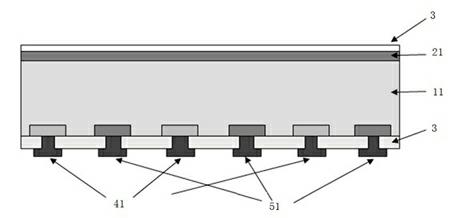
[0048] This example provides a process for fabricating a staggered back contact IBC battery by ion implantation, and the battery structure obtained is shown in the attached figure 2 shown, including the following steps:

[0049] (1) Suede corrosion

[0050] A p-type monocrystalline silicon substrate with a resistivity of 0.5-50 Ω·cm and a thickness of 50-500 is selected for surface texturing. For monocrystalline silicon substrates, surface texturing is carried out in 0.5~5% by weight sodium hydroxide deionized aqueous solution at a temperature of 75~90°C; for polycrystalline silicon substrates, surface texturing is carried out in nitric acid, hydrofluoric In the mixed solution of acid and deionized water with a volume ratio of 1~2:0.5~1:1, the surface texture is carried out under the condition of 5~15°C.

[0051] (2) Front ion implantation

[0052] Using the method of ion implantation, boron (B) doping is carried out on the front of the crystalline silicon substrate, the e...

Embodiment 2

[0068] This example provides a process for fabricating a staggered back contact IBC battery by ion implantation, and the battery structure obtained is as attached figure 2 shown, including the following steps:

[0069] (1) Suede corrosion

[0070] A p-type polysilicon substrate with a resistivity of 0.5-50 Ω·cm and a thickness of 50-500 is selected for surface texturing. For monocrystalline silicon substrates, surface texturing is carried out in 0.5~5% by weight sodium hydroxide deionized aqueous solution at a temperature of 75~90°C; for polycrystalline silicon substrates, surface texturing is carried out in nitric acid, hydrofluoric In the mixed solution of acid and deionized water with a volume ratio of 1~2:0.5~1:1, the surface texture is carried out under the condition of 5~15°C.

[0071] (2) Front thermal diffusion doping

[0072] The thermal diffusion doping method is used to do boron doping on the front side of the crystalline silicon substrate, the diffusion tempera...

Embodiment 3

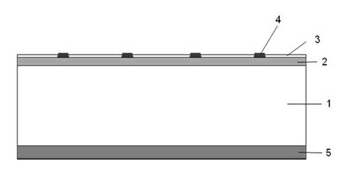
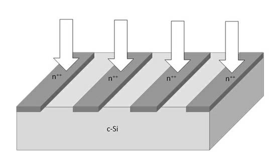
[0088] This example provides a process for fabricating staggered back-contact IBC cells by ion implantation, and the solar cell structure obtained is shown in the attached Figure 4 As shown, wherein 12 is an n-type silicon substrate, 22 is an n+ same-type doped layer, 3 is a passivation anti-reflection film, 42 is a p+ emitter, and 52 is an n+ base, including the following steps:

[0089] (1) Suede corrosion

[0090] Select an n-type single crystal silicon substrate with a resistivity of 0.5~50Ω·cm and a thickness of 50~500A for surface texturing. For monocrystalline silicon substrates, surface texturing is carried out in a sodium hydroxide solution with a weight percentage of 0.5~5% at a temperature of 75~90°C; for polycrystalline silicon substrates, surface texturing is carried out in nitric acid, hydrofluoric acid and In the mixed solution with the volume ratio of deionized water of 1~2:0.5~1:1, the surface texture is carried out under the condition of 5~15℃.

[0091] (2...


PUM

PropertyMeasurementUnit
electrical resistivityaaaaaaaaaa
thicknessaaaaaaaaaa
depthaaaaaaaaaa

Abstract

A technology for manufacturing an interlaced back contact (IBC) crystalline silicon solar battery with ion implantation comprises the following steps: (1) selecting a crystalline silicon base body to perform surface texturing; (2) forming a homotype doping layer having the same electrical property with the base body on the positive surface; (3) forming n+ doping regions and p+ doping regions interlaced to each other on the back surface of the crystalline silicon by the ion implantation; (4) insulating the n+ doping regions and the p+ doping regions on the back surface of the crystalline silicon base body; (5) performing annealing in order to eliminate crystalline damage caused by iron implantation to the crystalline silicon base body, and performing thermal oxidation to form a SiOx oxide layer; (6) forming a passive anti-reflecting film on the positive surface of a silicon chip; (7) forming a passive film on the back surface of the silicon chip; and (8) forming an emitter and a metal contact electrode of a base electrode on the back surface, and forming the ohmic contact of the metal electrode with the n+ doping regions and the p+ doping regions after one sintering. The method canaccurately control concentration, depth and position of the doping, and the technological process is simple, and easy to operate.

Description

technical field [0001] The invention belongs to the technical field of photovoltaics, and in particular relates to a process for manufacturing staggered back-contact IBC crystalline silicon solar cells by using an ion implantation method. Background technique [0002] Photovoltaic technology is a technology that uses large-area p-n junction diodes to convert solar energy into electrical energy. This p-n junction diode is called a solar cell. The semiconductor materials used to make solar cells have a certain band gap. When the solar cell is irradiated by the sun, photons with energy exceeding the band gap generate electron-hole pairs in the solar cell. The p-n junction separates the electron-hole pairs, and the p-n junction The asymmetry determines the flow direction of different types of photo-generated carriers, and the external power can be output through the external circuit connection. This is similar to the principle of ordinary electrochemical cells. figure 1 Give t...

Claims


Application Information

Patent Timeline
Patent Type & Authority Applications(China)
IPC IPC(8): H01L31/18
CPCY02P70/50
Inventor 蒋方丹周平蒋秀林汤坤单伟
Owner JA SOLAR TECH YANGZHOU
Why Eureka
Try Eureka