Preparation method of nano patterned sapphire substrate

A patterned sapphire and sapphire substrate technology, which is applied in chemical instruments and methods, nanotechnology, semiconductor/solid-state device manufacturing, etc., can solve the problems of expensive equipment, complicated process technology, high cost, etc., and achieve simple and repeatable preparation process Good, high yield effect

Inactive Publication Date: 2013-01-30
PEKING UNIV
View PDF5 Cites 15 Cited by
  • Summary
  • Abstract
  • Description
  • Claims
  • Application Information

AI Technical Summary

Problems solved by technology

[0004] Experiments have proved that the nanoscale patterned sapphire substrate (NanoPSS) can reduce the dislocation density of GaN more effectively than the traditional MPSS. At present, there are two ways to obtain nanoscale patterns. One is to pass electrons directly on the substrate. Beam exposure, deep ultraviolet lithography, laser interference and focused ion beam and other equipment. Although these methods can directly obtain the required pattern according to the design, if the complete 2-inch area is to be practical, the process technology involved is complicated. 1. The equipment is expensive and the efficiency is

Method used


Image

  • Preparation method of nano patterned sapphire substrate

Examples


Embodiment Construction

[0017] The present invention will be further described below in conjunction with the accompanying drawings and specific embodiments.

[0018] Referring to the accompanying drawings, a nanopillar patterned sapphire substrate is prepared according to the following process flow.

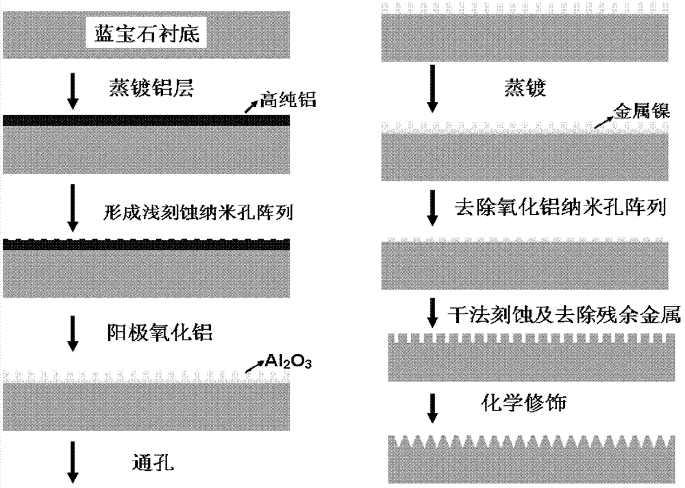
[0019] 1. Ultrasonic cleaning of sapphire with acetone, ethanol, and deionized water in sequence;

[0020] 2. Coating a high-purity aluminum layer on the surface of sapphire, wherein the metal aluminum layer can be prepared by electron beam evaporation, magnetron sputtering and electroplating, with a thickness of 300-2000 nanometers;

[0021] 3. Prepare a template with a nanostructure, specifically: prepare a 2-inch aluminum oxide nanostructure array template with a pore period of 460 nanometers by using the method of anodizing aluminum, and the conditions for anodic oxidation are: the oxidation voltage is 190V, and the electrolyte is The 0.1mol / L phosphoric acid solution and the reaction temperature a...


PUM


Abstract

The invention provides a preparation method of a nano patterned sapphire substrate, which comprises the following steps: firstly, cleaning a sapphire substrate, and coating a metal aluminum film on the surface by vaporization; meanwhile, preparing a template with a nano structure, and generating a corresponding pattern on the aluminum film by imprinting or etching; putting the sapphire substrate into an electrolyte solution to carry out anodization until the color on the aluminum film surface obviously changes and the current drops to 0, and making a through hole, thereby obtaining a patterned nano structure on the aluminum oxide layer; depositing a metal nickel layer; putting the sapphire substrate into a strongly alkaline solution to dissolve out the aluminum oxide layer, thereby obtaining a metal nickel nanodot matrix on the sapphire substrate; and etching the sapphire by using the metal nickel dot matrix as a mask, thereby obtaining a nano structure array with controllable depth on the sapphire substrate. The method of anodizing aluminum is utilized to obtain the highly-ordered nano structure array. Compared with the prior art, the invention has the advantages of simple preparation process, favorable repetitiveness and high yield.

Description

technical field [0001] The invention belongs to the technical field of preparation of GaN materials, in particular to a method for preparing a nanoscale patterned sapphire substrate. Background technique [0002] Gallium nitride (GaN) group III-nitrides are the most promising wide bandgap semiconductor materials, mainly including GaN, AlN, InN and their ternary and quaternary alloys. Due to its unique bandgap range, excellent photoelectric performance and good chemical stability, the material has made great progress in short-wavelength optoelectronic devices, especially GaN-based light-emitting diodes (LEDs) have been industrialized, and in Outdoor large-screen display, LCD backlighting, traffic lights, car tail lights, etc. are widely used. At the same time, it also opened the prelude to the revolution of the third-generation semiconductor material GaN-based semiconductor lighting. However, the quality of GaN crystals severely restricts the development and application of ...

Claims


Application Information

Patent Timeline
IPC IPC(8): H01L21/02C30B33/08B82Y40/00
Inventor 康香宁付星星章蓓于彤军陈志忠吴洁君杨志坚张国义
Owner PEKING UNIV
Why Eureka
Try Eureka