

Manufacturing method of two-dimensional ordered TiO2 nanometer well film and application in self-energized photoelectric device
A technology of optoelectronic devices and nanowells, which is applied in semiconductor/solid-state device manufacturing, nanotechnology, electrical components, etc., can solve the problems of limited reaction rate, insufficient strength, unstable photocurrent, etc., and achieve low cost, low cost, The effect of ultra-fast response speed
- Summary
- Abstract
- Description
- Claims
- Application Information
AI Technical Summary
Problems solved by technology
Method used
Image

Examples
Embodiment 1
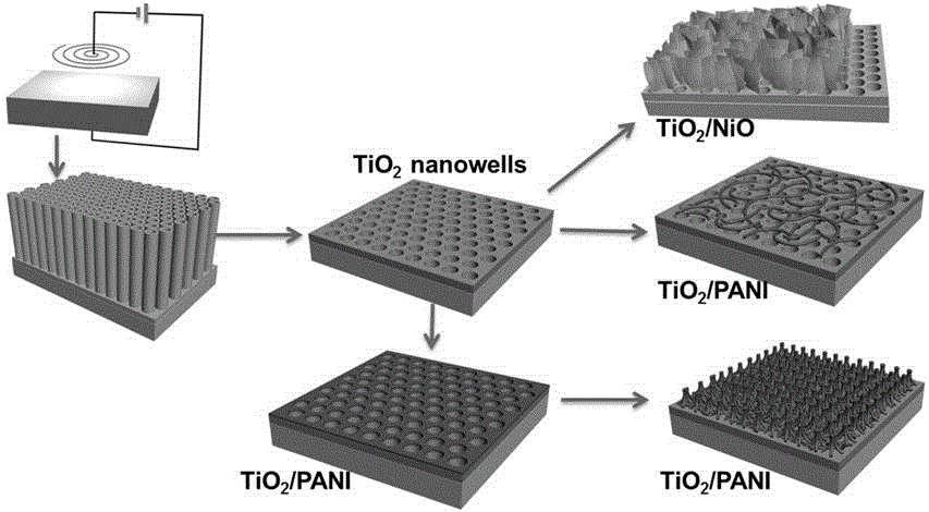
[0044] Embodiment 1, TiO 2 Fabrication of Nanowell Thin Films
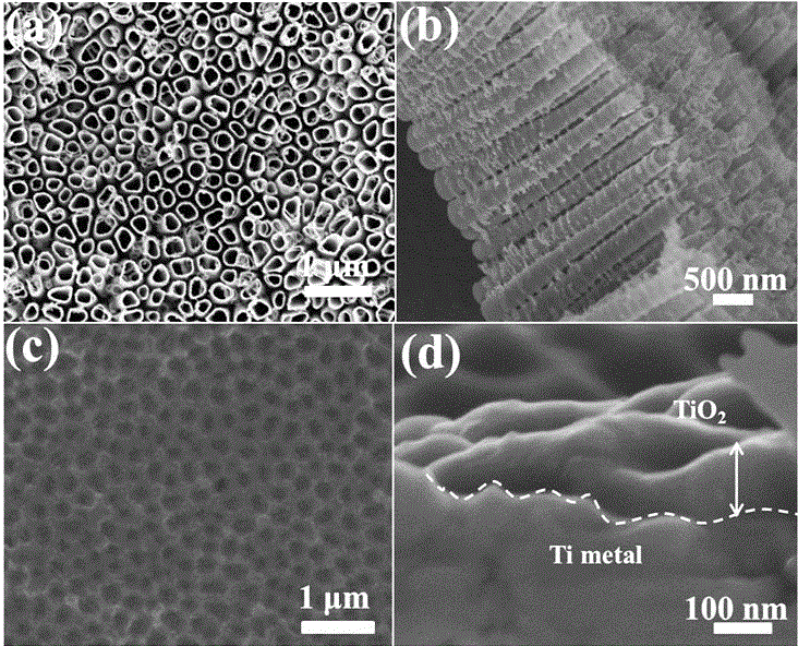
[0045] Take a 2cm×2cm titanium sheet with a purity of 99.6% as the anode, a platinum wire mesh as the cathode, and a mixture of 35wt% ammonium fluoride, 10% dimethyl sulfoxide and 85% lactic acid as the electrolyte, and apply 45 V voltage anodized for 12 hours to produce TiO 2 Nanotube array film (morphology see figure 2 , a~b); wash with a large amount of ethanol, dry with nitrogen, then tear off the prepared film with adhesive tape, wash with ethanol and dry with nitrogen; then place the titanium sheet in a muffle furnace for calcination, and the program is set as It was heated from room temperature to 450° C. within 85 minutes, kept at this temperature for 120 minutes, and then naturally cooled to room temperature. Take out the titanium sheet substrate to obtain anatase-type two-dimensional ordered TiO 2 Nanowell film (morphology see figure 2 , c~d).
[0046] Repeat the above steps, increase the voltage...
Embodiment 2
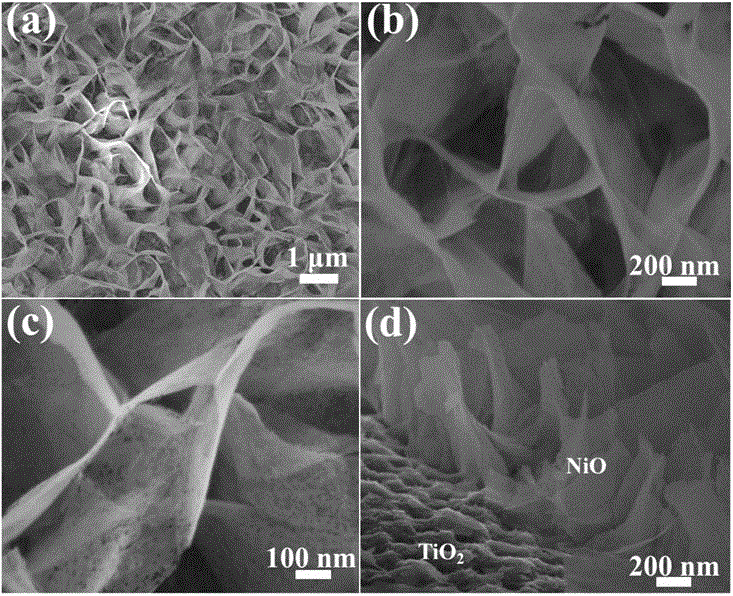
[0049] Embodiment 2, TiO 2 Preparation of / NiO Heterojunction Composite and Testing of Self-Energizing Properties of Photoelectric Devices
[0050] Take 57 mg of nickel chloride hexahydrate and 288 mg of urea respectively, and dissolve them in a glass bottle with a blue cap of 100 mL of deionized water. After stirring at room temperature for 10 minutes, the TiO prepared in Example 1 is 2 The nanowell film substrate was placed flat on the bottom of the glass bottle, then placed in an oven at 90°C for 24 hours, and cooled to room temperature naturally after the reaction. The substrate was taken out and rinsed with water three times, then placed in a muffle furnace for calcination. The program was set to heat from room temperature to 450°C within 140 minutes, and kept at this temperature for 120 minutes. After the heat preservation was completed, it was naturally cooled to room temperature. Taking out the substrate can make layered mesoporous NiO nanostructure and TiO 2 Nanowel...
Embodiment 3
[0054] Embodiment 3, TiO 2 / PANI heterojunction composite preparation
[0055] Prepare 20 mL of 1 M sulfuric acid aqueous solution containing 27.39 μL of aniline monomer in a beaker, and the TiO prepared in Example 1 2 The nanowell film substrate was placed flat on the bottom of the beaker, and another 20 mL of 1 M sulfuric acid aqueous solution containing 68.48 mg of ammonium persulfate was quickly poured along the wall of the beaker. After mixing, react at -5°C for 24 hours, then take out the substrate, wash it with water three times, place it in an oven at 60°C and dry it to obtain polyaniline film and TiO 2 Nanowell Composite TiO 2 / PANI (see Figure 5 , a~b).
[0056] Repeat the above steps and raise the reaction temperature to 10°C for 24 hours to obtain polyaniline fibers and TiO 2 Composite of nanowells (morphology see Figure 5 , c~d).
[0057] Repeat the above steps twice, using the prepared TiO 2 / PANI composite film is used as the substrate for secondary re...
PUM
| Property | Measurement | Unit |
|---|---|---|
| thickness | aaaaa | aaaaa |
| pore size | aaaaa | aaaaa |
| diameter | aaaaa | aaaaa |
Abstract
Description
Claims
Application Information