Method for planarization of potassium dihydrogen phosphate crystal optical surface
A potassium dihydrogen phosphate, optical surface technology, applied in chemical instruments and methods, crystal growth, single crystal growth and other directions, can solve the problems of low frequency error, high quality processing difficulty, brittleness, etc. Good mechanical properties and the effect of avoiding low frequency errors
- Summary
- Abstract
- Description
- Claims
- Application Information
AI Technical Summary
Problems solved by technology
Method used
Image

Examples
Embodiment 1
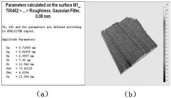
[0049] Including the following steps: (1) First use a single-point diamond lathe to measure 50×50×10mm 3 The Class I KDP crystal sample 1 was turned;
[0050] (2) Taking the sample 1 that has undergone single-point diamond turning as the processing object, and sputtering and depositing a layer of silicon film on the surface of the sample 1 by means of ion beam sputtering deposition; the target material of the film is silicon, and the target material is Specifications: 536×114×10.5mm;
[0051] Sputtering deposition time: 1h The main process parameters of planarization are controlled as follows:
[0052] Ion beam voltage 500V, ion beam current 150mA;
[0053] The ion beam accelerating voltage is 300V, and the ion beam accelerating current is 100mA;
[0054] Working gas: argon Gas flow rate: 35sccm;
[0055] Working pressure: 5.71E-2Pa ion beam incident angle 45°;
[0056] (3) Obtain a planarized layer by vacuum cooling, vacuum cooling: temperature 25°C, time 4h.
[0057] s...
Embodiment 2
[0062] Include the following steps:
[0063] (1) First use a single-point diamond lathe to cut to a size of 50×50×10mm 3 The Class I KDP crystal sample 2 was turned;
[0064] (2) Taking the sample 2 that has undergone single-point diamond turning as the processing object, use the method of ion beam sputtering to deposit a thin film on the surface of the sample 2 to sputter and deposit a layer of silicon film, the target specification: 536×114×10.5mm , the main process parameters of planarization are controlled as:
[0065] Ion beam voltage 500V, ion beam current 150mA;
[0066] The ion beam accelerating voltage is 300V, and the ion beam accelerating current is 100mA;
[0067] Working gas: Argon Gas flow rate: 35sccm;
[0068] Working pressure: 5.71E-2Pa, ion beam incident angle 45°, sputter deposition time 1.5h;
[0069] (3) Obtain a planarized layer by vacuum cooling. Vacuum cooling: temperature 25°C, time 4h.
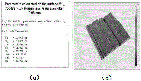
[0070] see image 3 , Figure 4 , using Talysurf CCI-20...
Embodiment 3
[0075] Include the following steps:
[0076] (1) First use a single-point diamond lathe to size 50×50×10mm 3 The Class I KDP crystal sample 3 was turned;
[0077] (2) Taking the sample 3 that has undergone single-point diamond turning as the processing object, use the method of ion beam sputtering to deposit a thin film on the surface of the sample 3 to sputter and deposit a layer of silicon film; target specification: 536×114×10.5 mm;
[0078] (3) Obtain a planarized layer by vacuum cooling.
[0079] The main process parameters of planarization are controlled as follows:
[0080] Ion beam voltage 500V, ion beam current 150mA;
[0081] The ion beam accelerating voltage is 300V, and the ion beam accelerating current is 100mA;
[0082] Working gas: Argon Gas flow rate: 35sccm;
[0083] Working pressure: 5.71E-2Pa ion beam incident angle 45°;
[0084] Sputtering deposition time 2h;
[0085] Vacuum cooling: temperature 25°C, time 4h.
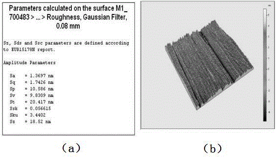
[0086] see Figure 5 , Figure 6 ,...
PUM
 Abstract
Description
Claims
Application Information
PatSnap Eureka turns technology decisions into work you can execute. Powered by our Innovation Knowledge Graph, it runs expert workflows across engineering, life sciences, materials and intellectual property. Get your review-ready output in minutes.


