

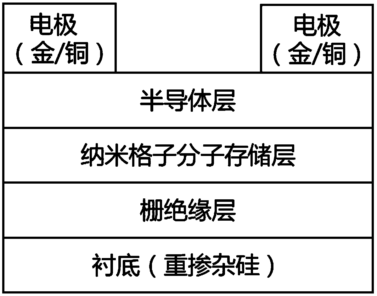
Organic field-effect transistor memory based on nano lattice molecules and preparation method thereof
A nano-lattice and molecular storage technology, applied in the fields of semiconductor/solid-state device manufacturing, organic chemistry, electric solid-state devices, etc., can solve the problems of difficult to achieve multi-level storage, poor device repeatability, poor data stability, etc., and achieve improved charge retention. Ability and Tolerance Ability, Reduced Manufacturing Cost, Low Cost Effect
- Summary
- Abstract
- Description
- Claims
- Application Information
AI Technical Summary
Problems solved by technology
Method used
Image

Examples
Embodiment 1
[0056] When X is C; Y is S; R is a linear octyloxy group, G1, G2, G3, and G4 are all hydrogen, and the lattice molecular structures are as follows:
[0057]
[0058] The synthetic route is as follows:
[0059]
[0060] The specific preparation method is as follows: dithiophene is obtained by coupling thiophene monomer through Pd / C catalysis, monobromofluorenone is obtained by Grignard reaction and Friedel-Crafts reaction to obtain compound 3, and the boronic acid of compound 3 and 2 in Pd(PPh 3 ) 4 Catalyst, alkali solution selection K 2 CO 3 Suzuki coupling under / KF conditions can efficiently obtain monosubstituted L-shaped precursors. The L-shaped precursor is in Et through its own dual active site tertiary alcohol group and the α position of thiophene. 2 O·BF 3 The catalyzed Friedel–Crafts reaction is closed to obtain nano-lattice molecules.
[0061] Compound 1: 2-bromothiophene (5.0 g, 30.6 mmol), 10% Pd / C (1.6 g, 1.5 mmol) was added 80 mL of anhydrous THF, protected by nitrogen...
Embodiment 2
[0067] The electrochemical determination of nano-grid molecular materials was measured in the CHI 660D electrochemical workstation of Shanghai Chenhua Instrument Company. The three-electrode system Pt electrode was used as the working electrode, the platinum wire was the auxiliary electrode, and the calomel electrode was the reference electrode. . Use 0.1M tetrabutyl fluoroborate (Bu 4 NPF 6 ) The acetonitrile solution is the electrolyte solution, ferrocene is used as the internal standard (0.40V), the electrolyte solution is blown into nitrogen for 20 minutes to remove oxygen, and the polymer chloroform solution is dripped on the working Pt electrode to form a film. Scanning during testing The speed is 50mV / s. According to the oxidation peak and reduction peak generated during the scanning process, the HOMO energy level and LUMO energy level can be calculated by analyzing the initial oxidation / reduction potential of the oxidation peak or reduction peak. Such as Figure 15 As ...
Embodiment 3
[0069] Thermogravimetric analysis (TGA) was performed on Shimadzu DTG-60H thermogravimetric analyzer, heating scanning speed was 10℃ / min and nitrogen flow rate was 20cm 3 / min. Differential scanning calorimetry (DSC) was performed on a Shimadzu DSC-60A tester. The sample was first heated at a rate of 10°C / min to a state where the decomposition temperature of the sample was ten degrees lower, and then, under liquid nitrogen The temperature is lowered back to the starting temperature, and the heating and heating scan is performed at a rate of 10°C / min for the second time. From the TGA experiment, the temperature at 5% weight loss (T d ) Are 458.05°C respectively. DSC experiment showed no obvious glass transition temperature.
PUM
| Property | Measurement | Unit |
|---|---|---|
| Thickness | aaaaa | aaaaa |
| Thickness | aaaaa | aaaaa |
| Thickness | aaaaa | aaaaa |
Abstract
Description
Claims
Application Information