A kind of perovskite photovoltaic cell and preparation method thereof
A perovskite battery and perovskite technology, applied in the field of solar cells, can solve problems such as battery stability degradation, achieve the effects of reducing interface defects, reducing costs, and reducing light absorption
- Summary
- Abstract
- Description
- Claims
- Application Information
AI Technical Summary
Problems solved by technology
Method used
Image
Examples
Embodiment 1
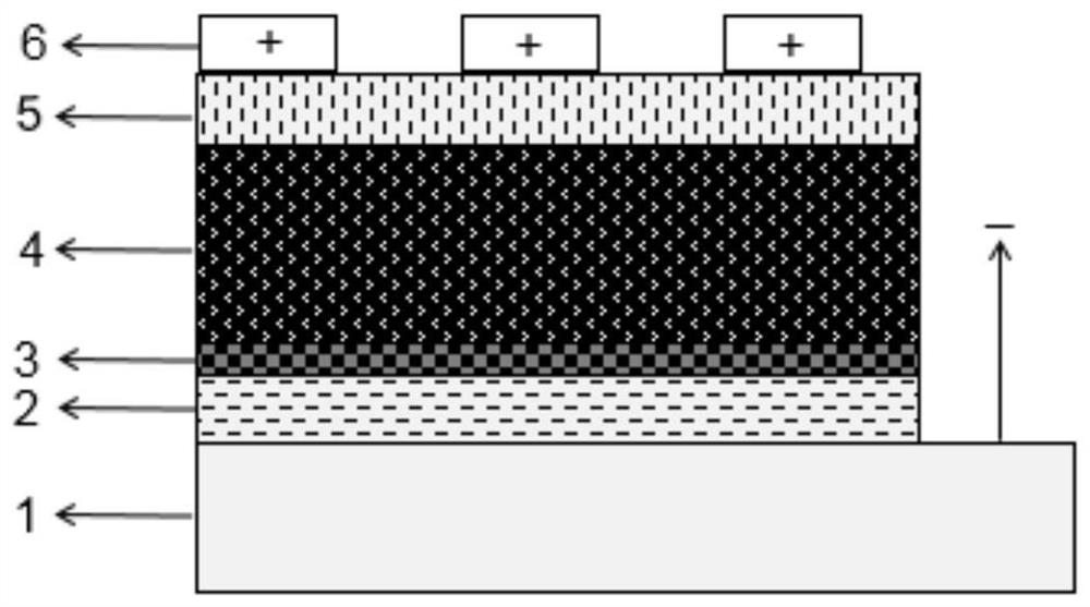
[0044] A planar structure perovskite photovoltaic cell, the schematic diagram is as follows figure 1 As shown, its structure includes a transparent conductive substrate 1, an electron transport layer 2, an interface passivation layer 3, a perovskite photoactive layer 4, a hole transport layer 5 and a metal electrode 6 from bottom to top, and the preparation method includes the following steps :
[0045] (1) Cleaning treatment of transparent conductive substrate: To clean the FTO conductive glass sheet, first soak the FTO conductive glass sheet in warm water containing detergent (such as liquid detergent) for 20 minutes, and then rinse it with clean water after repeated scrubbing; Then use polishing powder for polishing treatment; then put it into a vessel containing deionized water, acetone and alcohol for ultrasonic treatment for 20 minutes, and finally put it in deionized water to rinse twice, dry it with a nitrogen gun and put it in an oven Dry at 60℃;
[0046] (2) Prepar...
Embodiment 2
[0057] A planar structure perovskite photovoltaic cell, the structure of which includes a transparent conductive substrate, an electron transport layer, an interface passivation layer, a perovskite photoactive layer, a hole transport layer and a metal electrode from bottom to top, and the preparation method includes the following step:
[0058] (1) Cleaning the FTO conductive glass substrate: the same as in Example 1;
[0059] (2) Preparation of electron transport layer: SnO was prepared on FTO substrate 2 film, and put it into the ultraviolet ozone cleaning instrument for ultraviolet ozone treatment for 15 minutes, and quickly transfer the treated FTO substrate into the glove box;
[0060] (3) SnO on the substrate by solution method 2 Preparation of Fe on thin films 1.84 Mg 0.16 O 3 The thin film acts as an interface passivation layer;
[0061] a. Take 1mg of Fe 1.84 Mg 0.16 O 3 Add 2 ml of methanol to the particles, ultrasonically disperse for 2 times, each time for...
Embodiment 3
[0070] A planar structure perovskite photovoltaic cell, the structure of which includes a transparent conductive substrate, an electron transport layer, an interface passivation layer, a perovskite photoactive layer, a hole transport layer and a metal electrode from bottom to top, and the preparation method includes the following step:
[0071] (1) cleaning of ITO conductive glass substrate: same as Example 1;
[0072] (2) Preparation of electron transport layer: SnO was prepared on the cleaned ITO conductive glass substrate 2 Quantum dot film, put it into the UV-ozone cleaning instrument, and treat it with UV-ozone for 10 minutes in the atmospheric atmosphere and room temperature;
[0073] (3) SnO on the substrate by solution method 2 Preparation of Fe on Quantum Dot Films 1.80 Mg 0.20 O 3 The thin film acts as an interface passivation layer;
[0074] a. Take 1mg of Fe 1.80 Mg 0.20 O 3 Add 2 ml of methanol to the powder, ultrasonically disperse it twice for 30 minute...
PUM
| Property | Measurement | Unit |
|---|---|---|
| thickness | aaaaa | aaaaa |
| short-circuit current | aaaaa | aaaaa |
| short-circuit current | aaaaa | aaaaa |
Abstract
Description
Claims
Application Information


