Preparation method of high-thermal-conductivity diamond reinforced silicon carbide substrate

A diamond-enhanced, silicon carbide substrate technology, applied in semiconductor/solid-state device manufacturing, electrical components, circuits, etc., can solve the interface strength between SiC and diamond, thermal conductivity of nucleation defects, etching interface strength, interface thermal stress, etc. question

Active Publication Date: 2021-10-29
UNIV OF SCI & TECH BEIJING +1
View PDF7 Cites 8 Cited by
  • Summary
  • Abstract
  • Description
  • Claims
  • Application Information

AI Technical Summary

Problems solved by technology

Solve problems such as plasma etching, interface strength, interface thermal conductivity, and stress
Especially to solve the problem that the stress, SiC and diamond interface strength and nucleation defects affect the thermal conductivity of the SiC substrate that has been deposited with a thin layer of diamond in the process of SiC thinning or high temperature deposition of GaN on the SiC surface

Method used


Image

  • Preparation method of high-thermal-conductivity diamond reinforced silicon carbide substrate

Examples


specific Embodiment approach 1

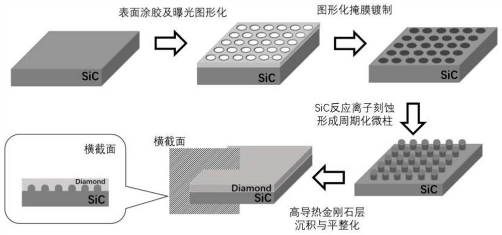
[0030] UV lithography is achieved by spin-coating photoresist on the carbon polar face of SiC and by mask-based. Then, periodic micropores with a diameter of 2 μm and an interval of 4 μm are realized by developing and degumming, revealing the periodically arranged diamond patterned surface. The SiC with the patterned photoresist is first deposited by electron beam evaporation with a Ti metal mask of 50nm and then an Al metal of 150nm. Then the remaining photoresist is removed to obtain the SiC with the metal pattern mask deposited on the surface. For SiC via gas source CF 4 :O 2 SiC was etched to an etching depth of 2 μm at a ratio of 5:1 and a bias power of 300 W. The metal mask is then removed by chemical dissolution. Subsequent passing SiC again through pure CF 4 The SiC was etched under the bias power of 20W to realize the rounded etching of the edge of the microcolumn. Then the patterned SiC sheet was placed in the microwave plasma chamber, the microwave power was c...

specific Embodiment approach 2

[0031] UV lithography is achieved by spin-coating photoresist on the carbon polar face of SiC and by mask-based. Then, periodic micropores with a diameter of 2 μm and an interval of 2 μm are realized by developing and degumming, revealing a periodically arranged diamond patterned surface. The SiC with patterned photoresist was first deposited with 30nm of Ti metal mask and then 120nm of Al metal by electron beam evaporation. Then the remaining photoresist is removed to obtain the SiC with the metal pattern mask deposited on the surface. For SiC via gas source CF 4 :O 2 SiC was etched to an etching depth of 1 μm at a ratio of 4:1 and a bias power of 200 W. The metal mask is then removed by chemical dissolution. Subsequent passing SiC again through pure CF 4 The SiC was etched under the bias power of 10W to realize the rounded etching of the edge of the microcolumn. Then the patterned SiC sheet was placed in the microwave plasma chamber, the microwave power was controlled ...

specific Embodiment approach 3

[0032] UV lithography is achieved by spin-coating photoresist on the carbon polar face of SiC and by mask-based. Then, periodic micropores with a diameter of 5 μm and an interval of 8 μm are realized by developing and degumming, and the periodically arranged diamond patterned surface is exposed. The SiC with patterned photoresist is first deposited with a Ti metal mask of 40 nm and then deposited with an Al metal of 150 nm by electron beam evaporation. Then the remaining photoresist is removed to obtain the SiC with the metal pattern mask deposited on the surface. For SiC via gas source CF 4 :O 2 SiC was etched to an etching depth of 3 μm at a ratio of 2:1 and a bias power of 100 W. The metal mask is then removed by chemical dissolution. Subsequent passing SiC again through pure CF 4 The SiC was etched under the bias power of 10W to realize the rounded etching of the edge of the microcolumn. Then the patterned SiC sheet was placed in the microwave plasma cavity, the micr...


PUM

PropertyMeasurementUnit
thermal conductivityaaaaaaaaaa
electrical resistivityaaaaaaaaaa

Abstract

The invention discloses a preparation method of a high-thermal-conductivity diamond enhanced silicon carbide (SiC) substrate, and belongs to the field of semiconductor material preparation. According to the invention, the method comprises the steps: patterning the carbon polar surface of SiC through gluing, photoetching and developing; performing electron beam evaporation or magnetron sputtering on a metal mask; after the photoresist is removed, performing reactive ion etching, mask removal and secondary ion etching on the SiC with the periodically arranged metal mask to obtain the micro-column array; growing a diamond layer through a microwave plasma chemical vapor deposition technology; after the diamond layer completely covers the micro-column and has a certain thickness, performing laser scanning leveling and subsequent precision polishing to obtain the high-thermal-conductivity diamond enhanced SiC substrate. The heat conduction efficiency is improved by increasing the effective contact interface area of diamond and SiC, and meanwhile, insufficient bonding force and local defect expansion of a single plane interface are effectively avoided. And a foundation is laid for obtaining SiC / Diamond and GaN / SiC / Diamond wafers for high power and high frequency by thinning a SiC silicon polar surface and depositing GaN on the surface of the SiC silicon polar surface at high temperature in the future.

Description

technical field [0001] The invention belongs to the field of semiconductor material preparation and relates to a preparation method of a high thermal conductivity diamond reinforced silicon carbide substrate. Background technique [0002] Silicon carbide (SiC) and gallium nitride (GaN), as a wide bandgap semiconductor, are ideal materials for radio frequency and power devices. In the development of future technologies such as photovoltaic industry, high-speed trains, electric vehicles, 5G radio frequency, satellite communications and radar will play an increasingly important role. High strength and hardness, high thermal shock resistance and corrosion resistance make SiC excellent in extreme temperature environments. In addition, as a representative third-generation semiconductor material, SiC can be used as high-power, high-frequency electronic devices in harsh environments by taking advantage of its wide bandgap and high dielectric breakdown electric field strength. Howe...

Claims


Application Information

Patent Timeline
Patent Type & Authority Applications(China)
IPC IPC(8): H01L21/04H01L21/3065H01L21/308
CPCH01L21/0475H01L21/3086H01L21/3065
Inventor 郑宇亭李成明张钦睿刘思彤魏俊俊郝志恒刘金龙陈良贤安康张建军
Owner UNIV OF SCI & TECH BEIJING
Why Eureka
Try Eureka