Circuit board, circuit board manufacturing method and display apparatus provided with circuit board

A technology of circuit substrate and manufacturing method, which is applied in the direction of printed circuit manufacturing, circuit, circuit cover, etc., and can solve problems such as material degradation

Inactive Publication Date: 2007-04-11
ZEON CORP +1
View PDF17 Cites 5 Cited by
  • Summary
  • Abstract
  • Description
  • Claims
  • Application Information

AI Technical Summary

Problems solved by technology

However, when the method of the above-mentioned JP-A-6-69190 is carried out as it is, hydrofluoric acid is generated, and the organic material or silicon-based substrate material is degraded by the generated hydrofluoric acid.

Method used


Image

  • Circuit board, circuit board manufacturing method and display apparatus provided with circuit board
  • Circuit board, circuit board manufacturing method and display apparatus provided with circuit board
  • Circuit board, circuit board manufacturing method and display apparatus provided with circuit board

Examples


Embodiment

[0107] Examples of the present invention are described below. In addition, this invention is not limited to the following Examples. In addition, the analysis values ​​in the following examples and comparative examples are all values ​​obtained by rounding off, and "parts" represent "parts by weight".

[0108] In addition, the analysis conditions in the following examples and analysis examples are as follows.

[0109] (Test 1) Temperature rise detachment analysis (hereinafter abbreviated as "TDS analysis".)

[0110] Device: EMD-WA1000S / W manufactured by Electronic Science Corporation

[0111] (Test 2) Fourier transform infrared spectrophotometric analysis (hereinafter abbreviated as "FT-IR analysis".)

[0112] Installation: Spectrum One, PerkinElmer

[0113] (Test 3) Cavity Ring Drop Spectroscopy (hereinafter abbreviated as "CRDS analysis".)

[0114] Device: MTO-1000H2O manufactured by Tiger Optics

[0115] (Test 4) Measurement of contact angle

[0116] Device: CA-D made...

manufacture example 1

[0124] [Adjustment of thermosetting photosensitive resin composition (positive type)]

[0125] The 8-hydroxycarbonyltetracyclo[4.4.0.1 2,5 1 7,10 ] 62.5 parts of dodec-3-ene, 37.5 parts of N-phenyl (5-norbornene-2,3-dicarboxyimide), 1.3 parts of 1-hexene, 1,3 dimethylimidazoline - 2-indene (tricyclohexylphosphine) benzylidene, 0.05 parts of ruthenium chloride and 400 parts of tetrahydrofuran were installed in a nitrogen-substituted glass pressure-resistant reactor, and reacted at 70°C for 2 hours while stirring to obtain a polymer Product solution A (solid concentration about 20%).

[0126] Part of this polymer solution A was transferred into an autoclave with a stirrer, and hydrogen was dissolved and reacted for 5 hours at 150° C. with a pressure of 4 MPa to obtain a polymer solution B containing a hydrogenated polymer (hydrogenation rate 100%) (Concentration of solid content: about 20%).

[0127] A heat-resistant container in which a part of activated carbon powder was a...

manufacture example 2

[0130] [Adjustment of thermosetting photosensitive resin composition (negative type)]

[0131] 300.0 parts of methyltrimethoxysilane, 47.5 parts of conductivity are 8×10 -5 S cm -1 The ion-exchanged water and 0.1 part of oxalic acid were put into a container with a stirrer, and heated and stirred at 60° C. for 6 hours to hydrolyze methyltrimethoxysilane. Then, after adding 1,000 parts of propylene glycol monomethyl ether into the container, ion-exchanged water and hydrolyzed by-product methanol were removed using an evaporator to obtain a solution adjusted to a solid content of 25% by weight.

[0132] After 400 parts of the above solution and 2.0 parts of phenyl 4-(2'-hydroxy-1'-tetradecyloxy)phenyliodonium-p-toluenesulfonate as a radiation-sensitive acid generator were uniformly mixed and dissolved, Filtration was performed with a membrane filter having a pore diameter of 0.2 μm to obtain a thermosetting photosensitive resin composition.


PUM


Abstract

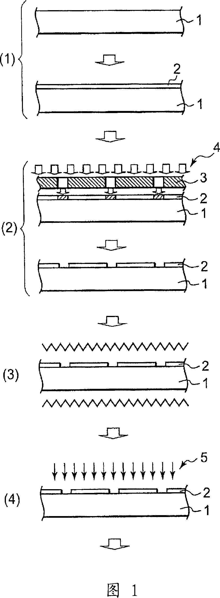
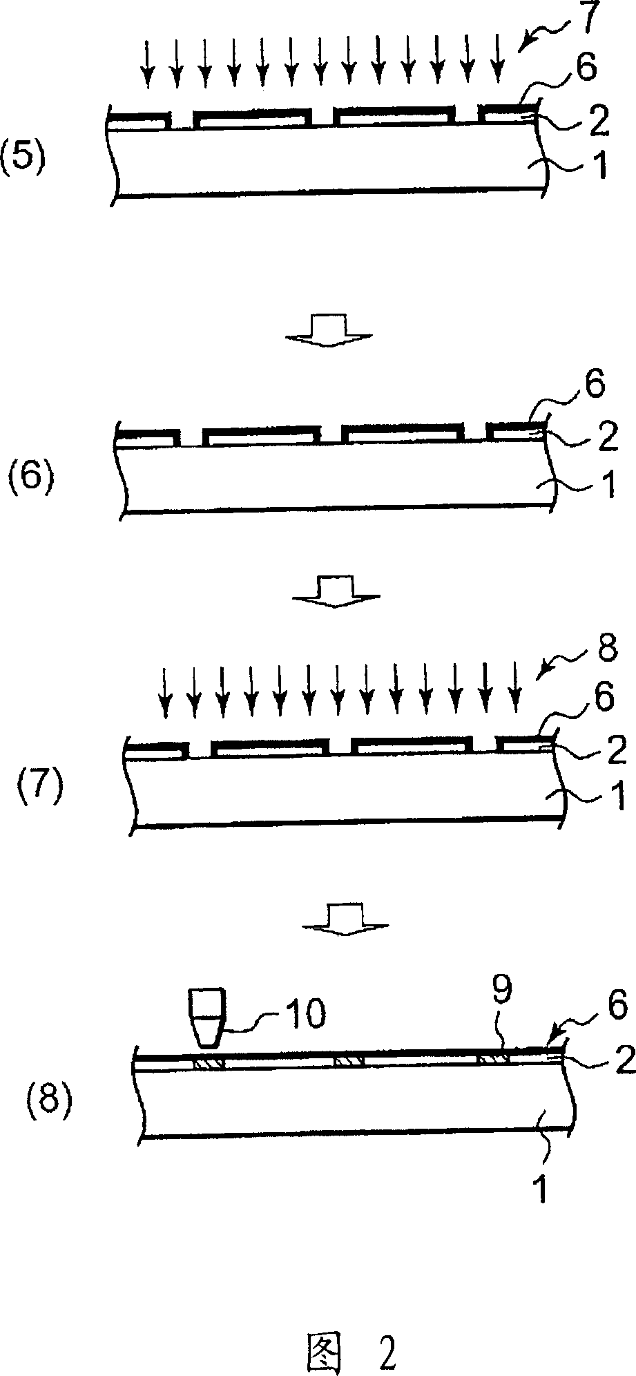
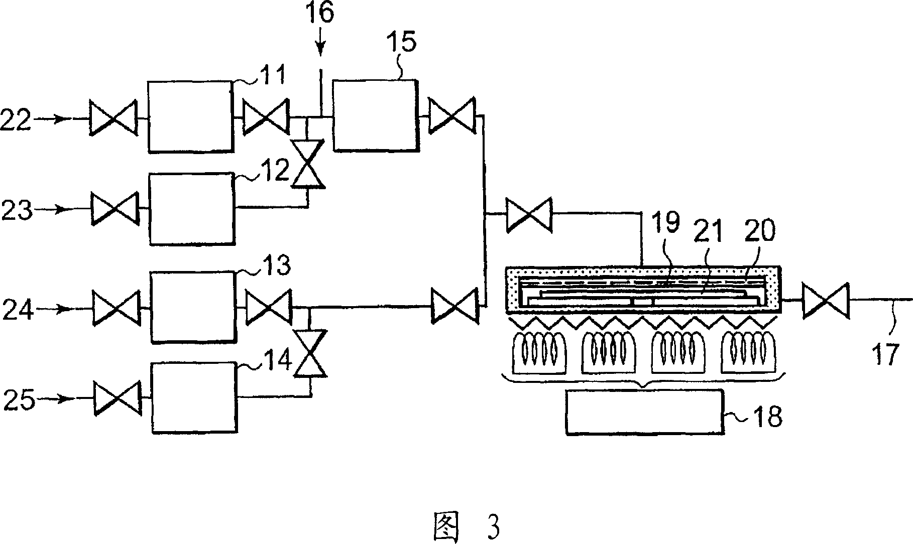
A circuit board manufacturing method includes formation of a thermosetting photosensitive resin film on an insulating board by a spin coat method and the like, exposure of the photosensitive resin film to radiation rays such as ultraviolet rays, development with a developer or by etching, heat-hardening of the photosensitive resin film, oxygen plasma treatment or ultraviolet treatment if required, adjustment of a water quantity in the photosensitive resin film by drying the resin film, exposure in a fluorine gas atmosphere, anneal treatment, and then immersion of the resin film in a fluorinated acid chemical.

Description

technical field [0001] The present invention relates to a circuit board useful for electrical and electronic applications, a method for manufacturing the circuit board, and a display device having the circuit board. Background technique [0002] The substrate for electronic equipment is to arrange a plurality of thin film transistors in a single layer or in multiple layers on an insulating substrate such as glass or resin or a substrate formed of an insulator at least on the surface; Or an electrical wiring layer connected between input and output terminals. [0003] A typical embodiment of a substrate for electronic equipment is a display device such as an active matrix liquid crystal display device or an organic EL display device. The whole substrate including scanning lines, signal lines, etc. is called an active matrix substrate, and it is composed of several layers of circuit patterns formed on the surface of the substrate by film formation or photolithography in a red...

Claims


Application Information

Patent Timeline
Patent Type & Authority Applications(China)
IPC IPC(8): H05K3/10H05B33/14G02F1/1362G03F7/40H01L21/48H05K3/00H05K3/12H05K3/18
CPCH05K2203/0568H05K3/1258H05K3/184G03F7/40H05K2203/095H05K3/0023H05K3/1241H05K2203/087H01L21/481H05K3/0073G02F2001/136295G02F1/136295Y10T29/49155G02F1/13H05K3/10
Inventor 大见忠弘二井启一铃木辉彦加藤丈佳
Owner ZEON CORP
Why Eureka
Try Eureka