Silicon single crystal, silicon wafer, and epitaxial wafer

a single crystal, silicon wafer technology, applied in the direction of silicon compounds, water-setting substance layered products, transportation and packaging, etc., can solve the problems of increasing leakage current, increasing leakage current, and shortening the life of the carrier,

Inactive Publication Date: 2002-10-03
SUMITOMO MITSUBISHI SILICON CORP
View PDF0 Cites 17 Cited by
  • Summary
  • Abstract
  • Description
  • Claims
  • Application Information

AI Technical Summary

Benefits of technology

[0017] In consideration of the gettering effect induced by crystal defects in an OSF ring region, the present inventors have conducted a variety of studies directed toward conditions that increase the width of an OSF ring, and have found that doping of nitrogen during Czochralski growth of a single crystal increases the width of the ring. Thus, when the entire surface of a wafer serves as an OSF region, nuclei of precipitates that are difficult to extinguish during an epitaxial process and stable at high temperature effectively function as gettering sites.
[0019] Thus, the present inventors have studied conditions for increasing the width of OSF rings and generating crystal defects attributed to the rings on the entire surface of a wafer, as well as for increasing the effectiveness of the gettering effect, and have found that when nitrogen serves as a single dopant and is doped in an amount of 1.times.10.sup.18 atoms / cm.sup.3 or more, nuclei of OSF are produced and diffused in an amount effective for attaining homogeneous gettering in a single crystal. In addition, when a Si epitaxial layer is formed on the surface of a slice obtained from the single crystal, there is produced a wafer having very few surface defects and exhibiting effective gettering action in a step for producing a device.
[0022] The above-described gettering method is particularly effective for wafers used in a p-, n-, or n+ device in which precipitate nuclei for forming sinks are easily extinguished by a step for forming an epitaxial layer. In addition, the method is also effective for a p+ wafer doped at high concentration with boron which getters Fe and effectively getters an element other than Fe.
[0023] The gettering effect for the epitaxial-layer-formed wafer is evaluated by MOS generation lifetime. The present inventors have conducted further, detailed investigation of wafers exhibiting excellent results among the thus-nitrogen-doped wafers, and have found that generation of OSF is observed at a density of 10.sup.2 / cm.sup.2 or more at a surface of substrate after a thermal oxidation treatment. Briefly, when a single crystal possesses defect nuclei, which produce OSF at a certain density or more through the thermal oxidation treatment, an excellent gettering effect may be attained.
[0024] The epitaxial layer is preferably formed on a wafer, which is heated to 1000.degree. C. or higher. When a wafer sliced from a nitrogen-doped single crystal is heated to 1000.degree. C. or higher, a temperature similar to that used for formation of the epitaxial layer, defects are observed at a density of 5.times.10.sup.4 / cm.sup.2 or more in a cross-section. Such defects serve as sinks for gettering to thereby enhance the gettering effect of a wafer, and are obtained from defects nuclei generated in a single crystal by nitrogen doping.
[0025] However, a variety of device processes are carried out after an epitaxial process, and the history of the heat treatment of a wafer varies in accordance with the device processes, such as a low-temperature device process which is mainly carried out at a temperature of 800.degree. C. or less, and a high-temperature device process which is mainly carried out at a temperature greater than 800.degree. C. When a low-temperature device process is employed, oxide precipitate nuclei, which are not extinguished during an epitaxial process but remain thereafter, grow at a speed lower than that in the case of a high-temperature device process, to thereby yield insufficient gettering capability. In order to solve the problem, the present inventors have found that carbon or boron, which enhance the formation rate and the growth rate of oxide precipitates, is doped in addition to nitrogen even in a low-temperature device process, to thereby ensure excellent gettering capability.

Problems solved by technology

As the integration density of silicon semiconductor integrated circuit devices rapidly increases, a silicon wafer from which devices are formed is subjected to increasingly severe specifications.
Thus, since circuits are made thinner with increasing integration density within a device active region wherein a device is formed on a wafer, crystal defects, such as dislocations and elemental metal impurities other than a dopant, which increase leakage current and shorten the life of a carrier are subjected to more rigorous limitations than ever before.
Although oxygen is effective for enhancing the strength of a silicon wafer by preventing generation of dislocations and for providing a gettering effect, oxygen is well known to deposit in the form of an oxide and to induce crystal defects such as dislocation or a stacking fault caused by heating during production of a device.
Therefore, oxygen diffuses slowly, and formation of the above-mentioned denuded zone is insufficient.
Even though reduction of oxygen content in a substrate has been attempted, crystal defects are insufficiently suppressed and the performance of a wafer is deteriorated by the reduction in oxygen content.
Thus, attempts to reduce oxygen content have yielded unsatisfactory results.
However, contamination with elemental metal impurities exerts a strong influence, because a complicated process is required for realizing high-density integration and contamination occurs frequently.
Although purification of the production environment and raw materials is essential for preventing contamination, complete prevention of contamination in the process of producing the device is difficult.
Therefore, a crystal defect is intentionally introduced to thereby capture and confine impurities.
Of the above-mentioned gettering techniques, extrinsic gettering represented by imparting distortion to a reverse side of a wafer involves drawbacks such as an increase in production costs due to addition of production steps; generation of particles due to detachment of silicon chips from a portion imparted with distortion; and warp of a wafer resulting from the treatment.
Furthermore, in an epitaxial wafer substrate, oxide precipitates which are to serve as nuclei of micro-defects shrink to disappear due to employment of a temperature as high as 1050-1200.degree. C. during a step for forming an epitaxial layer, to thereby disturb subsequent formation of sinks during heat treatment.
Particularly, as mentioned above, when a device process is carried out at relatively low temperature, the growth rate of oxide precipitates decreases to disadvantageously result in an insufficient gettering effect to metal impurities at an initial stage of the device process as well as during the entire course of the step.
However, other drawbacks remain, such as a long-duration heat treatment and complex processing steps.
As described hereinabove, a heat treatment carried out before and after an epitaxial process may introduce problems, such as decrease in productivity and increase in costs due to an increase in the number of steps; damage to a boat during the treatment; and a reduction in yield due to particle generation.
OSF is a stacking fault generated in a crystal under an oxide film during a high-temperature oxidation treatment in a device process.
However, such disclosed methods are directed toward preventing dislocations or preventing deterioration in withstand voltage, and effects of these methods on gettering and the shape of OSF rings have remained unknown.
When a low-temperature device process is employed, oxide precipitate nuclei, which are not extinguished during an epitaxial process but remain thereafter, grow at a speed lower than that in the case of a high-temperature device process, to thereby yield insufficient gettering capability.

Method used


Image

  • Silicon single crystal, silicon wafer, and epitaxial wafer
  • Silicon single crystal, silicon wafer, and epitaxial wafer
  • Silicon single crystal, silicon wafer, and epitaxial wafer

Examples


example 1

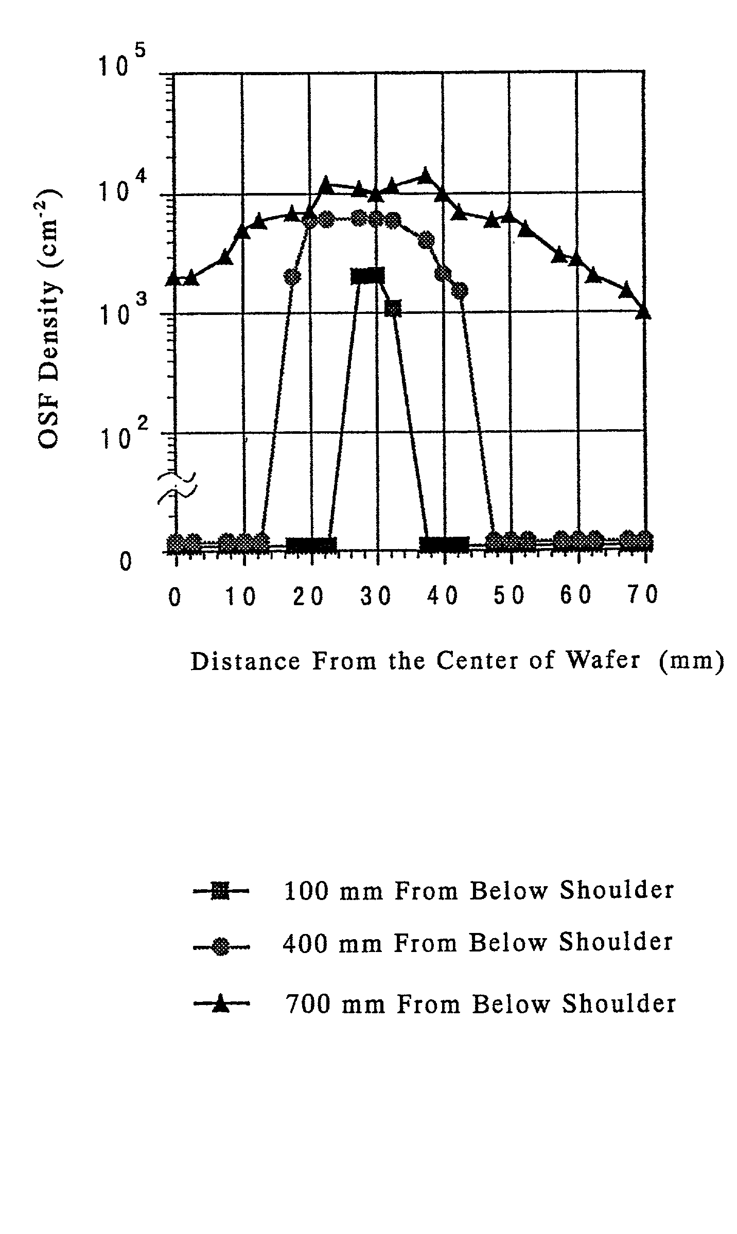
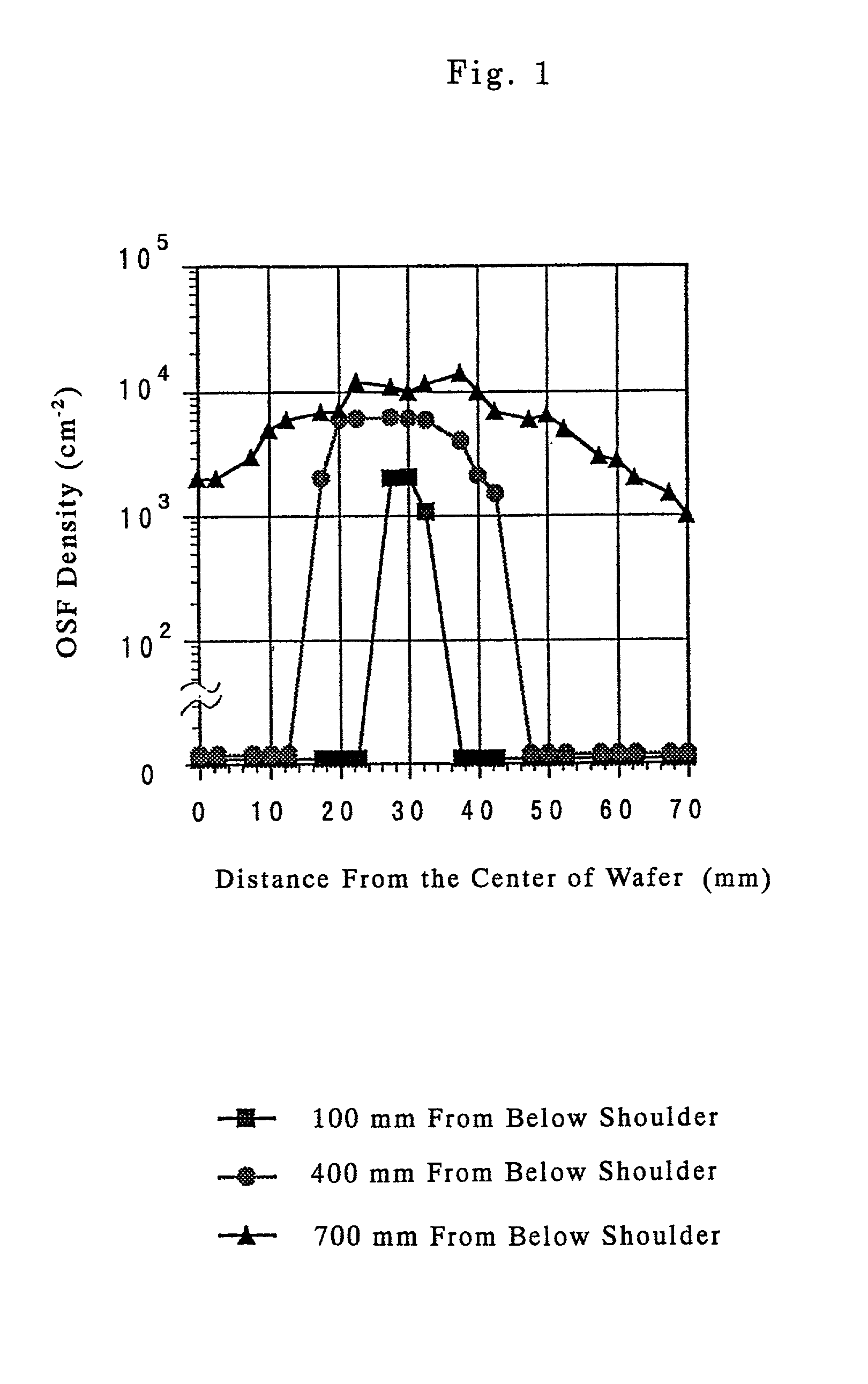
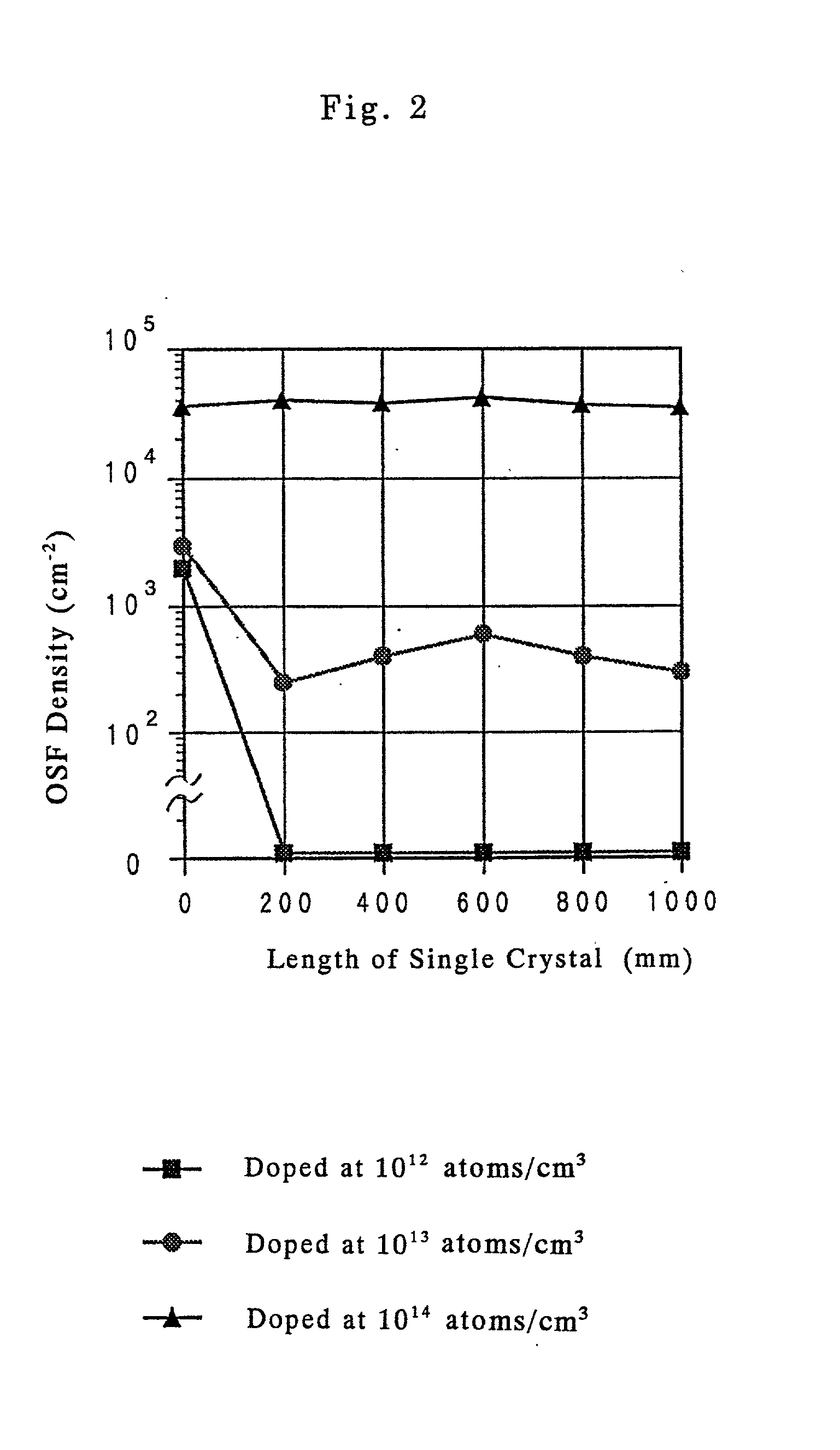
[0050] According to the Czochralski method, a single crystal was grown in the following manner; i.e., highly pure poly-crystalline silicon (50 kg) was melted in a quartz crucible along with boron serving as a dopant, and the single crystal having a diameter of 150 mm and a crystal orientation of was pulled at a pulling speed of 0.6 mm / min.

[0051] First, in order to clarify the effect of nitrogen, nitrogen gas was blown into the crucible at a rate of 10 l / min in order to increase nitrogen concentration in the crystal during the crystal growth step, when a single crystal was grown to a length of 300 mm below a shoulder. Next, in order to easily assume a nitrogen doping concentration, three grades of nitrogen-doped single crystals having respective doping concentrations of 10.sup.12 atoms / cm.sup.3, 10.sup.13 atoms / cm.sup.3, and 10.sup.14 atoms / cm.sup.3 were grown by melting a silicon wafer having a silicon nitride layer possessing a predetermined nitrogen content together with highly p...

example 2

[0055] On the single crystal silicon wafer doped with nitrogen at a concentration of 10.sup.14 atoms / cm.sup.3 in Example 1, an approximately 5-.mu.m-thick epitaxial layer was formed at a deposition temperature of 1150.degree. C. The thus-obtained wafer was then subjected to selective etching in a wright etchant for 5 minutes. The defect densities on the surface and the cross sections of the epitaxial layer were determined under an optical microscope.

[0056] FIG. 3 shows the defect densities on the surface and cross sections at various radial distances from the center of the specimens. After formation of the epitaxial layer, defects are present at a density of approximately 1.times.10.sup.4 / cm.sup.2 along the cross sections of nitrogen-doped single crystal silicon wafer under the epitaxial layer. This indicates that oxide precipitates may not be diminished during formation of the epitaxial layer at high temperature. However, defects were observed on neither the surface nor the cross s...

example 3

[0057] Nitrogen doping was carried out at respective concentrations of 0, 10.sup.12 atoms / cm.sup.3, 10.sup.13 atoms / cm.sup.3, and 10.sup.14 atoms / cm.sup.3, on two types of wafer substrates; more specifically, on a wafer substrate having a high electric resistance of 10 .OMEGA..multidot.cm and on a wafer substrate having a low electric resistance of 0.008 .OMEGA..multidot.cm. From the thus-obtained eight types of single crystals, wafer substrates were sliced and subjected to deposition at 1150.degree. C. to form an epitaxial layer having a thickness of approximately 5 .mu.m.

[0058] These wafers were contaminated with a 3 ppm aqueous solution of Cu(NO.sub.3).sub.2 by use of a spin coater, then subjected to a heat treatment in a dry oxygen atmosphere as a model treatment simulating the device production process, to thereby investigate the change in the gettering effect during heat treatment.

[0059] FIG. 4 shows a temperature-time profile of the model heat treatment. At the three time poi...


PUM

PropertyMeasurementUnit
temperatureaaaaaaaaaa
thicknessaaaaaaaaaa

Abstract

There are provided silicon single crystal, silicon wafer, and epitaxial wafer having a sufficient gettering effect suitable for a large-scale integrated device. The silicon single crystal which is suitable for an epitaxial wafer is grown with nitrogen doping at a concentration of 1x10¹³ atoms / cm3 or more, or with nitrogen doping at a concentration of 1x10¹² atoms / cm3 and carbon doping at a concentration of 0.1x10¹⁶-5x10¹⁶ atoms / cm3 and / or boron doping at a concentration of 1x10¹⁷ atoms / cm3 or more. The silicon wafer is produced by slicing from the silicon single crystal, and an epitaxial layer is grown on a surface of the silicon wafer to produce the epitaxial wafer. The present invention provides an epitaxial wafer for a large-scale integrated device having no defects in a device-active region and having an excellent gettering effect without performance of an extrinsic or intrinsic gettering treatment, which is a factor for increasing the number of production steps and production costs.

Description

[0001] The present invention relates to a silicon single crystal used for a semiconductor integrated circuit device and to a silicon wafer and an epitaxial wafer, which are obtained therefrom and used for forming an integrated circuit. More particularly, the present invention relates to a silicon single crystal, a silicon wafer, and an epitaxial wafer exhibiting high gettering capability which is provided by doping with nitrogen solely, or with nitrogen and carbon and / or boron during growth of a single crystal and without provision of an additional step.DESCRIPTION OF THE PRIOR ART[0002] As the integration density of silicon semiconductor integrated circuit devices rapidly increases, a silicon wafer from which devices are formed is subjected to increasingly severe specifications. Thus, since circuits are made thinner with increasing integration density within a device active region wherein a device is formed on a wafer, crystal defects, such as dislocations and elemental metal impur...

Claims


Application Information

Patent Timeline
Patent Type & Authority Applications(United States)
IPC IPC(8): C30B15/00H01L21/208C30B29/06H01L21/02
CPCC30B15/00Y10T428/21C30B29/06
Inventor ASAYAMA, EIICHIHORAI, MASATAKAMURAKAMI, HIROKIKUBO, TAKAYUKIUMENO, SHIGERUSADAMITSU, SHINSUKEKOIKE, YASUOSUEOKA, KOUJIKATAHAMA, HISASHI
Owner SUMITOMO MITSUBISHI SILICON CORP
Why Eureka
Try Eureka