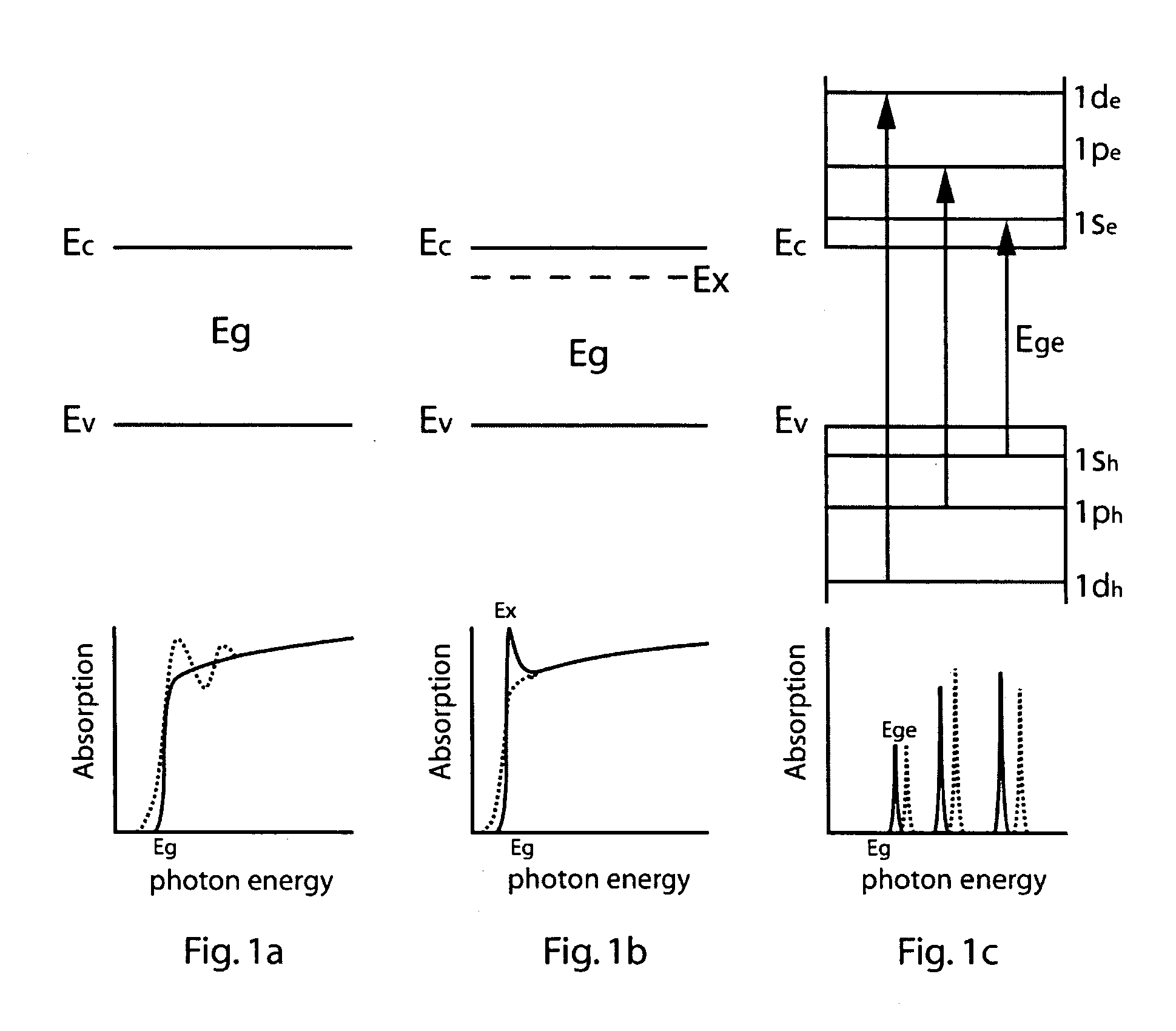
[0008] A common approach to achieve optical modulation in a
semiconductor material is to apply an electrical field with, e.g., an applied
voltage to modify the width of the band-gap. One example of this is the Franz-Keldysh effect, which change the
band gap directly by applied field. The
electron-hole pair created by the
photon forms an entity that resembles a
hydrogen atom and is called an "
exciton". In an
exciton, the
Coulomb attraction between the
electron and hole lowers the energy of the
electron relative to the
conduction band edge. The excitonic interaction changes the allowed states of the electrons (
conduction band) and holes (
valence band). An applied
electric field modifies or even counters the excitonic interaction, changing the allowed states around the band edge. This, in turn, changes the optical absorption of photons that have energy near the band-gap. The lowest energy where absorption occurs is called the
absorption edge. In a sample where at least one dimension is comparable to the
exciton size, this effect is also called
quantum confined
stark effect.
[0015] where E.sub.g is the band-gap for the bulk, E.sub.x is the exciton ground energy for the bulk value, m.sub.e and m.sub.h are the effective masses of the electron and hole respectively, h is the
Plank constant and .
omega. is the
angular frequency of the
photon. This formula treats the excitons
Coulomb interaction as a
hydrogen-like entity. The last term in this equation indicates that the absorption peak energy corresponding to the exciton increases rapidly with
size reduction.
[0039] Due to the
confined space, the probability of direct recombination of the electron and hole, a radiative process in which a photon is emitted, is much reduced. Because of the small spatial dimension of the nano-particles,
momentum conservation can be violated in particle interactions. Removing
momentum conservation and including the increased overlapping of electron and hole wave functions make non-radiative many particle process, such as
Auger recombination, more likely to happen. The exciton recombines through phonons rather than photons. The non-radiative recombination can make some optical devices, such as a modulator, more efficient, since there is less "
stray light" being emitted by the device.
[0040] The handling and
processing of nano-particles can be more economical than thin film growth. For example, in GaAs, to enhance the exciton energy by
quantum confinement, fabrication and optimization of a
multiple quantum well (MQW) by
metal-organic
chemical vapor deposition (MOCVD) or
molecular beam epitaxy (MBE) is employed. These processes are expensive and complicated. In addition, not all semiconductors can be made into MQW presently. Issues like suitable substrates, growth conditions, thermal budget, and strains can limit the final performance of the devices. Nano-particles can be synthesized and assembled by chemical methods on literally any substrate. These chemical processes are potentially cheaper and more forgiving than MOCVD and MBE. The particles experience no or little strain, thereby reducing the complications associated with thin film hetero-structures. Plus, a greater variety of semiconductors can potentially be made in the form of nano-particles. Finally, using bulk-form semiconductors can limit material choices, where one has to select from a limited number of materials to operate at a given photon
wavelength. For example, to work at UV wavelengths, some materials such as Si and GaAs may not be desirable because their band-gaps are too small. However, one can potentially engineer a, for example, GaAs nano-particle for UV applications by simply making the GaAs nano-particle small enough.
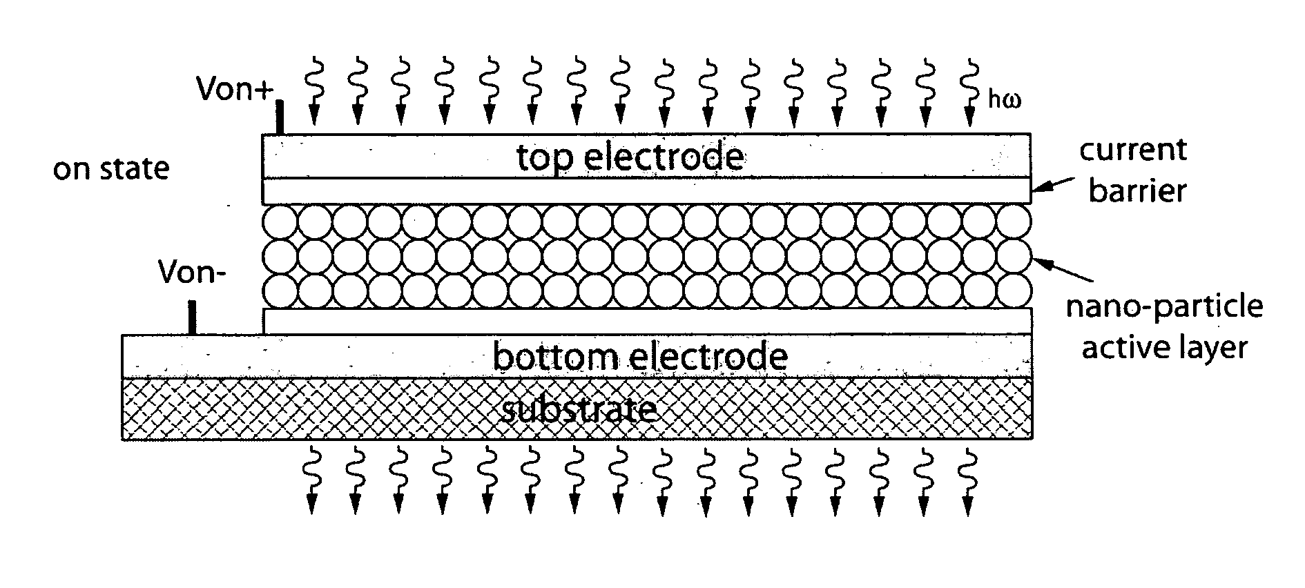
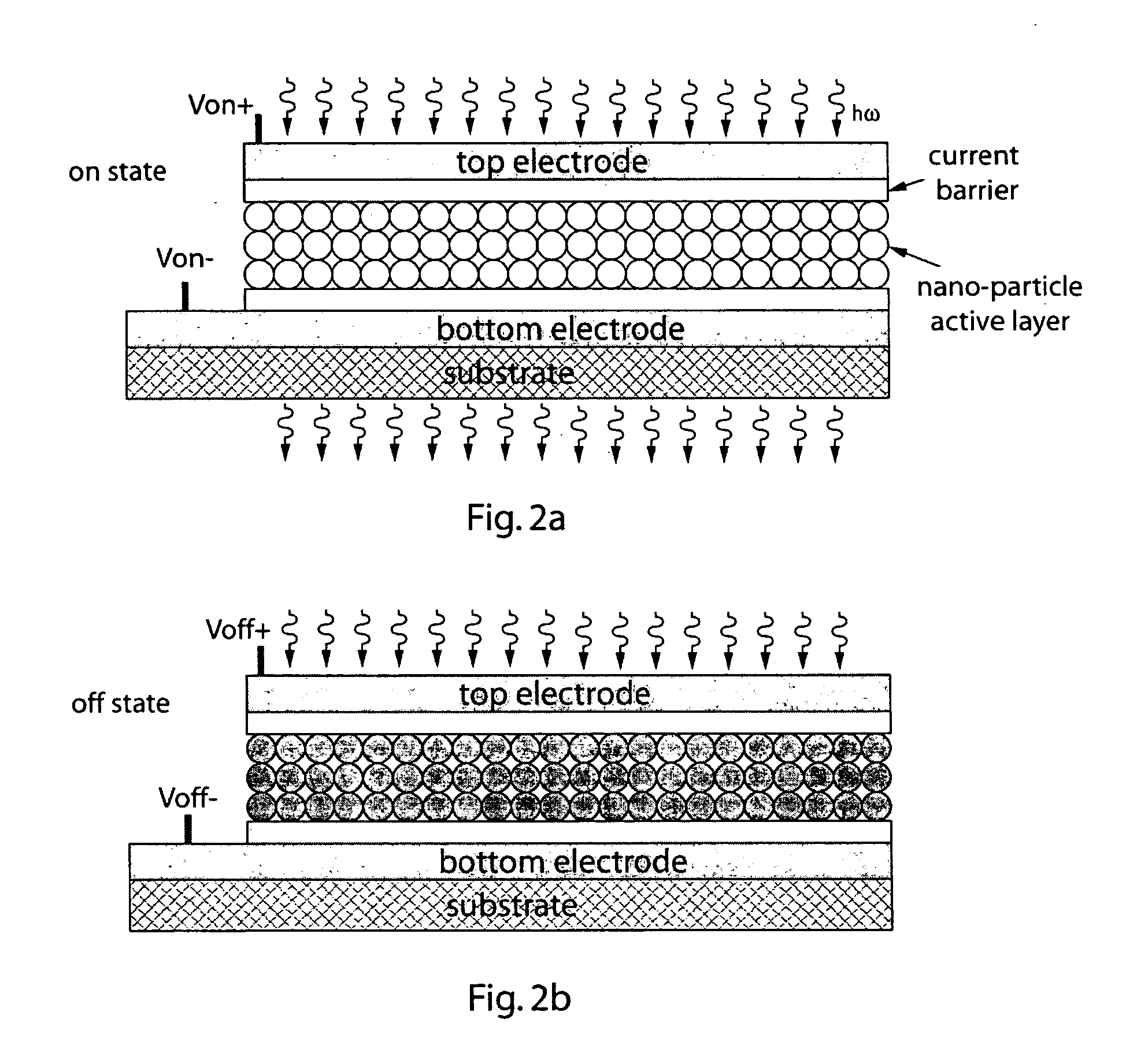
[0041] Nano-particles can be synthesized and handled at
room temperature or slightly elevated temperatures. This is exceptionally appealing for integration with
silicon circuit. No
special care has to be taken to reduce the thermal budget. This
advantage offers simplicity in the embodiments for programmable
photolithography masks where large arrays of optical modulators are integrated with
silicon control circuit The indispensable requirement of programmable lithographic
mask is densely integrated optical modulators operating at high speed, high uniformity and high reliability.

