Wire bonding process for copper-metallized integrated circuits

a technology of integrated circuits and wire bonding, which is applied in the direction of semiconductor devices, semiconductor/solid-state device details, electrical apparatus, etc., can solve the problems of significant technological challenges, pronounced aluminum sensitivity to electromigration becoming a serious obstacle, and the relative high resistivity of interconnecting aluminum now appears inferior to the lower resistivity of metals such as copper, so as to avoid the cost of new capital investment and prevent excessive copper up-diffusion

Inactive Publication Date: 2005-05-19
TEST HOWARD R +2
View PDF30 Cites 5 Cited by
  • Summary
  • Abstract
  • Description
  • Claims
  • Application Information

AI Technical Summary

Benefits of technology

[0016] Another object of the invention is to use only designs and processes most commonly employed and accepted in the fabrication of IC devices, thus avoiding the cost of new capital investment and using the installed fabrication equipment base.
[0017] These objects have been achieved by the teachings of the invention concerning selection criteria and process flows suitable for mass production. The non-oxidized surface of the copper of the bond pad is seeded by a metal such as palladium and covered with a layer of a barrier m

Problems solved by technology

Consequently, the relatively high resistivity of the interconnecting aluminum now appears inferior to the lower resistivity of metals such as copper.
Further, the pronounced sensitivity of aluminum to electromigration is becoming a serious obstacle.
From the standpoint of the mature aluminum interconnection technology, however, this shift to copper is a significant technological challenge.
For bond pads made of copper, the formation of thin copper(I)oxide films during the manufacturing process flow has to be prevented, since these films severely inhibit reliable attachment of bonding wires, especially for conventional gold-wire ball bonding.
In contrast to aluminum oxide films overlying metallic aluminum, copper oxide films overlying metallic copper cannot easily b

Method used


Image

  • Wire bonding process for copper-metallized integrated circuits
  • Wire bonding process for copper-metallized integrated circuits
  • Wire bonding process for copper-metallized integrated circuits

Examples


Embodiment Construction

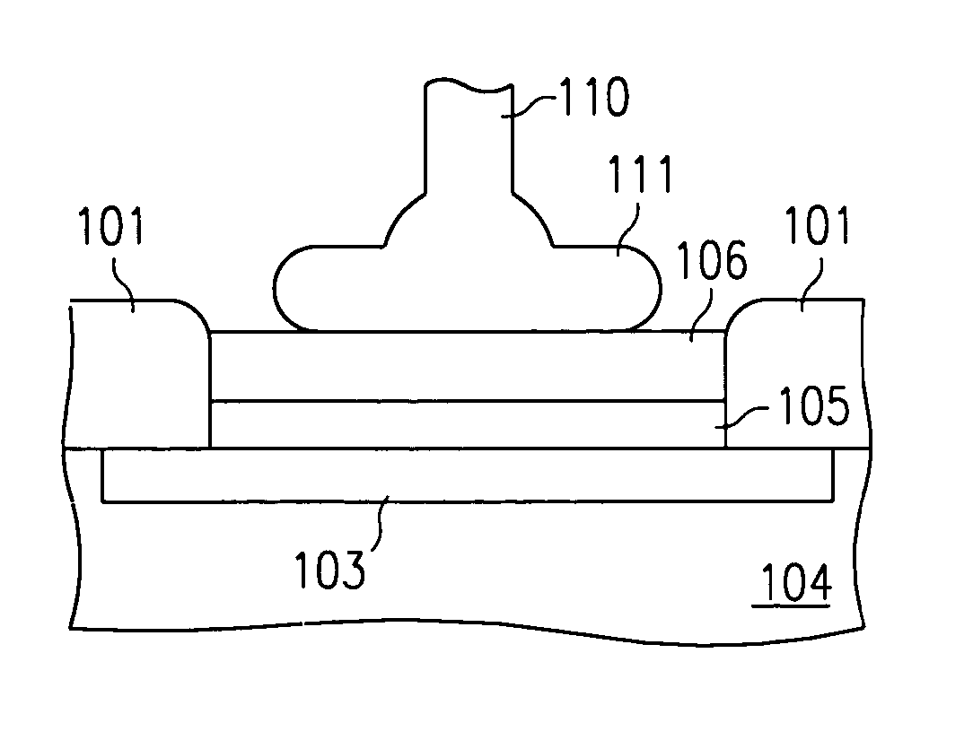
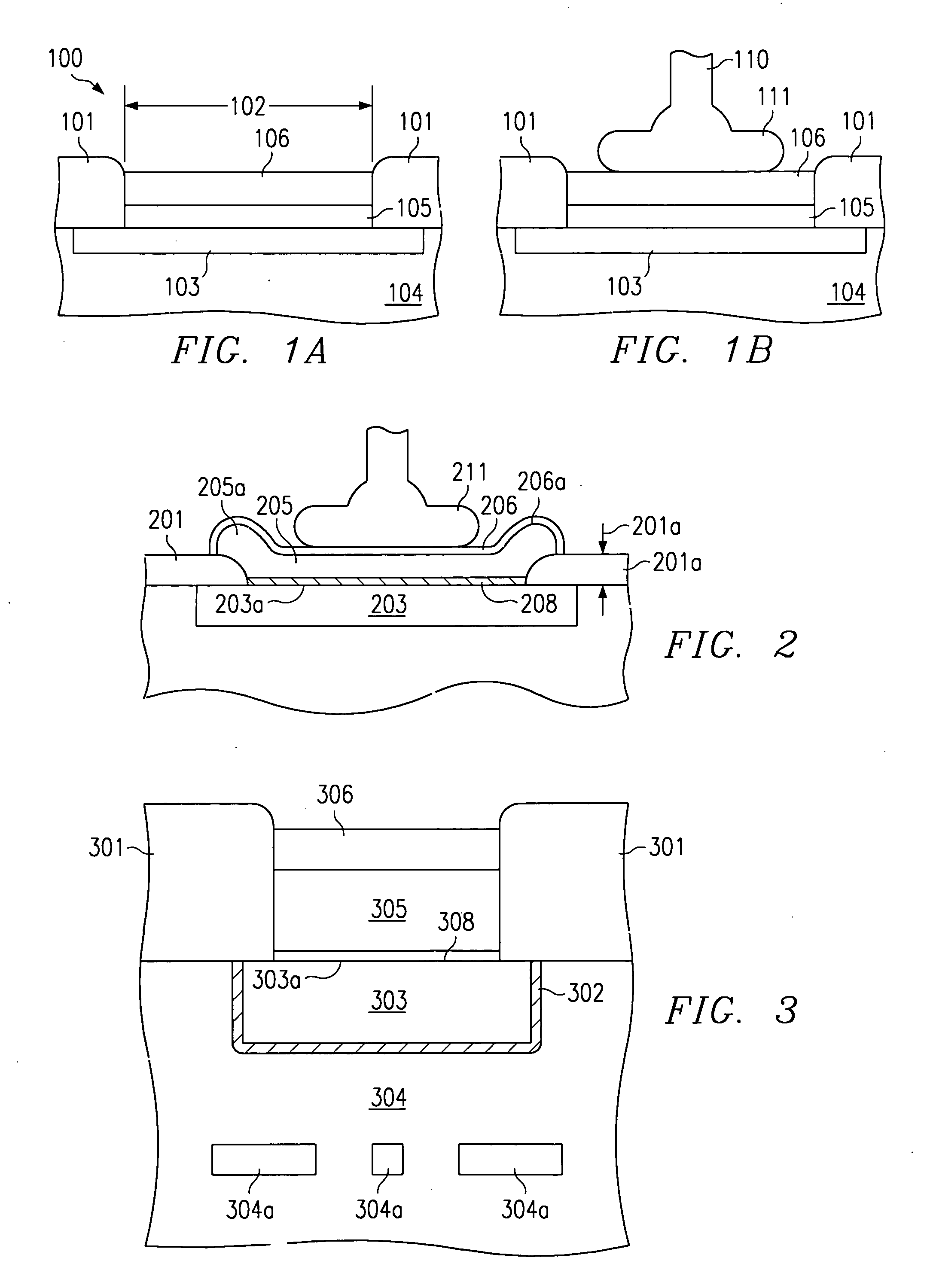
[0026]FIG. 1A shows a schematic cross section of the preferred embodiment of the invention, generally designated 100. An integrated circuit (IC) has copper interconnecting metallization and is covered by a moisture-impenetrable protective overcoat 101. This overcoat is usually made of silicon nitride, commonly 0.5 to 1.0 μm thick. A window 102 is opened in the overcoat in order to expose portion of the copper metallization 103. Not shown in FIG. 1A is the underlayer embedding the copper and preventing its diffusion into parts of the IC (usually made of tantalum nitride, tantalum silicon nitride, tungsten nitride, tungsten silicon nitride, titanium, titanium nitride, or titanium tungsten; see FIG. 3).

[0027] In FIG. 1A, the dielectric IC portions 104 are only summarily indicated. These electrically insulating portions may include not only the traditional plasma-enhanced chemical vapor deposited dielectrics such as silicon dioxide, but also newer dielectric materials having lower diel...


PUM


Abstract

A robust, reliable and low-cost metal structure and process enabling electrical wire/ribbon connections to the interconnecting copper metallization of integrated circuits. The structure comprises a layer of barrier metal that resists copper diffusion, deposited on the non-oxidized copper surface in a thickness such that the barrier layer reduces the diffusion of copper at 250° C. by more than 80% compared with the absence of the barrier metal. The structure further comprises an outermost bondable layer which reduces the diffusion of the barrier metal at 250° C. by more than 80% compared with the absence of the bondable metal. Finally, a metal wire is bonded to the outermost layer for metallurgical connection. The barrier metal is selected from a group consisting of nickel, cobalt, chromium, molybdenum, titanium, tungsten, and alloys thereof. The outermost bondable metal layer is selected from a group consisting of gold, platinum, and silver.

Description

BACKGROUND OF THE INVENTION [0001] The present invention is related in general to the field of semiconductor devices and processes and more specifically to the process of wire bonding to bond pads of copper-metallized integrated circuits. DESCRIPTION OF THE RELATED ART [0002] In integrated circuits (IC) technology, pure or doped aluminum has been the metallization of choice for interconnection and bond pads for more than four decades. Main advantages of aluminum include easy of deposition and patterning. Further, the technology of bonding wires made of gold, copper, or aluminum to the aluminum bond pads has been developed to a high level of automation, miniaturization, and reliability. Examples of the high technical standard of wire bonding to aluminum can be found in U.S. Pat. No. 5,455,195, issued on Oct. 3, 1995 (Ramsey et al., “Method for Obtaining Metallurgical Stability in Integrated Circuit Conductive Bonds”); U.S. Pat. No. 5,244,140, issued on Sep. 14, 1993 (Ramsey et al., “...

Claims


Application Information

Patent Timeline
IPC IPC(8): H01L23/52H01L21/288H01L21/3205H01L21/60H01L23/485H01L23/532
CPCH01L21/288H01L23/53233H01L23/53238H01L24/03H01L24/05H01L24/45H01L24/48H01L24/85H01L2224/04042H01L2224/05082H01L2224/05111H01L2224/05147H01L2224/05155H01L2224/05157H01L2224/05164H01L2224/05166H01L2224/05171H01L2224/0518H01L2224/05184H01L2224/05624H01L2224/05639H01L2224/05644H01L2224/05647H01L2224/05655H01L2224/05664H01L2224/05669H01L2224/0568H01L2224/45014H01L2224/45015H01L2224/45124H01L2224/45144H01L2224/45147H01L2224/4845H01L2224/48463H01L2224/85013H01L2224/85201H01L2224/85205H01L2924/01004H01L2924/01006H01L2924/01013H01L2924/01014H01L2924/01022H01L2924/01027H01L2924/01028H01L2924/01029H01L2924/01033H01L2924/01042H01L2924/01046H01L2924/01047H01L2924/0105H01L2924/01073H01L2924/01074H01L2924/01075H01L2924/01078H01L2924/01079H01L2924/01327H01L2924/014H01L2924/04941H01L2924/04953H01L2924/05042H01L2924/10253H01L2924/14H01L2924/19043H01L2924/20751H01L2924/20752H01L2924/20753H01L2924/3025H01L2924/00014H01L2924/01005H01L2924/01024H01L2924/01076H01L2224/48624H01L2224/48644H01L2224/48647H01L2224/48655H01L2224/48664H01L2224/48669H01L2224/48839H01L2224/48844H01L2224/48847H01L2224/48855H01L2224/48864H01L2224/48639H01L2224/4868H01L2224/48724H01L2224/48739H01L2224/48747H01L2224/48755H01L2224/48764H01L2224/48769H01L2224/4878H01L2224/05556H01L2224/78H01L2924/00H01L2224/48824H01L2224/48869H01L2224/48744H01L2224/4888H01L2224/78252H01L2224/78253H01L2224/85203H01L2924/206H01L21/60
Inventor TEST, HOWARD R.AMADOR, GONZALOSUBIDO, WILLMAR E.
Owner TEST HOWARD R
Why Eureka
Try Eureka