Method for manufacturing semiconductor device
a manufacturing method and semiconductor technology, applied in semiconductor devices, instruments, photosensitive materials, etc., can solve the problems of unsuitable mass production, high production cost, and low yield of substrates, and achieve excellent impact resistance properties and high yield
- Summary
- Abstract
- Description
- Claims
- Application Information
AI Technical Summary
Benefits of technology
Problems solved by technology
Method used
Image

Examples
embodiment mode 1
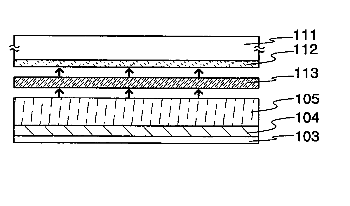
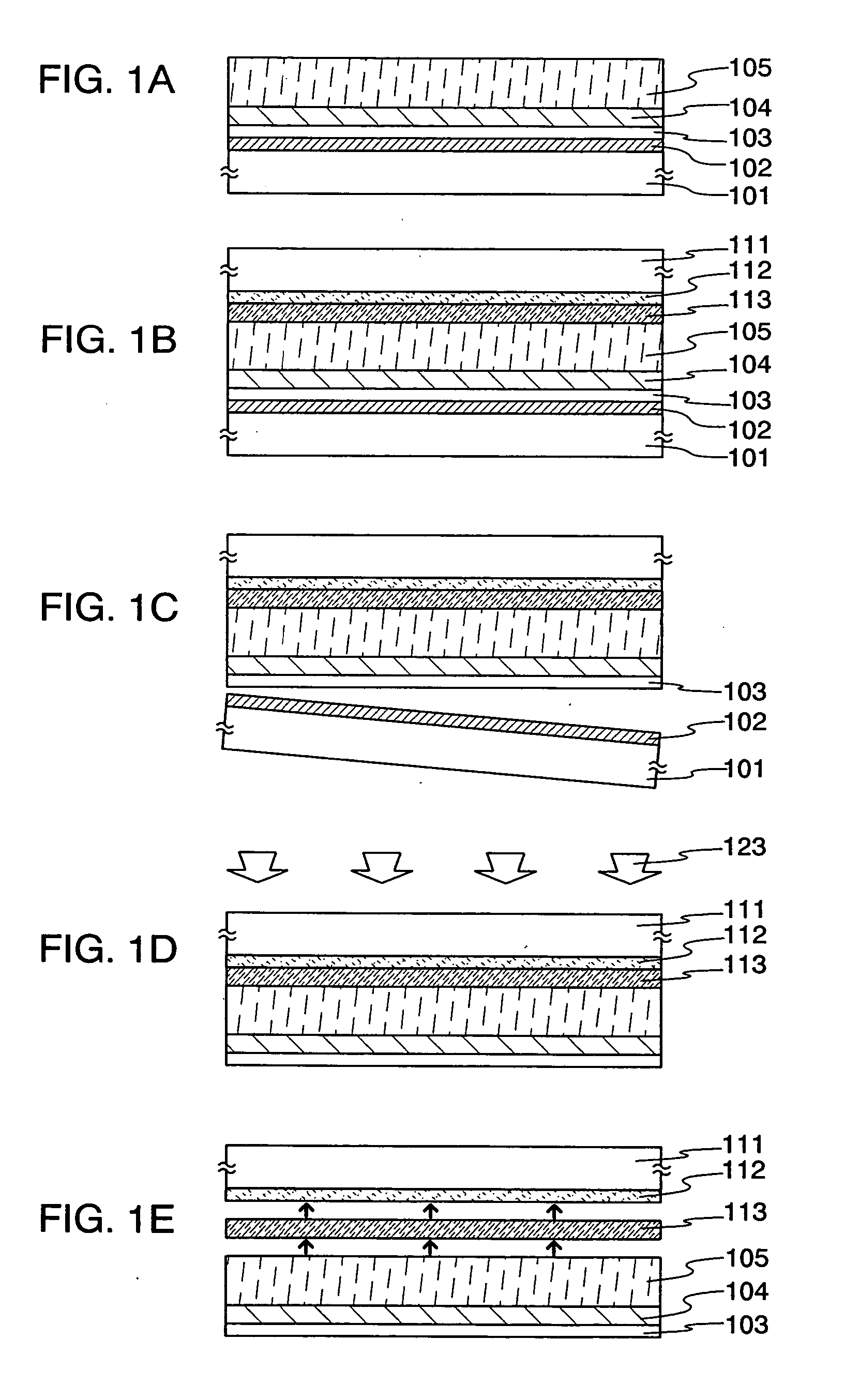
[0043] In the present embodiment mode, a method of separating a lamination body formed over a substrate will be described with reference to FIGS. 1A to 1E.
[0044] As shown in FIG. 1A, a metal film 102 is formed on a first substrate 101. As the first substrate, a heat-resistant substrate, i.e., a material that can withstand the heat treatment in a step of manufacturing an optical filter formed later and the separation step, typically, a glass substrate, a quartz substrate, a ceramic substrate, a silicon substrate, a metal substrate, or a stainless substrate can be used.
[0045] The metal film 102 may be formed of an element selected from titanium (Ti), aluminum (Al), tantalum (Ta), tungsten (W), molybdenum (Mo), copper (Cu), chromium (Cr), neodymium (Nd), iron (Fe), nickel (Ni), cobalt (Co), ruthenium (Ru), rhodium (Rh), palladium (Pd), osmium (Os), iridium (Ir); a single layer formed of an alloy material containing the above-mentioned elements as its main constituent; or a lamination...
embodiment mode 2
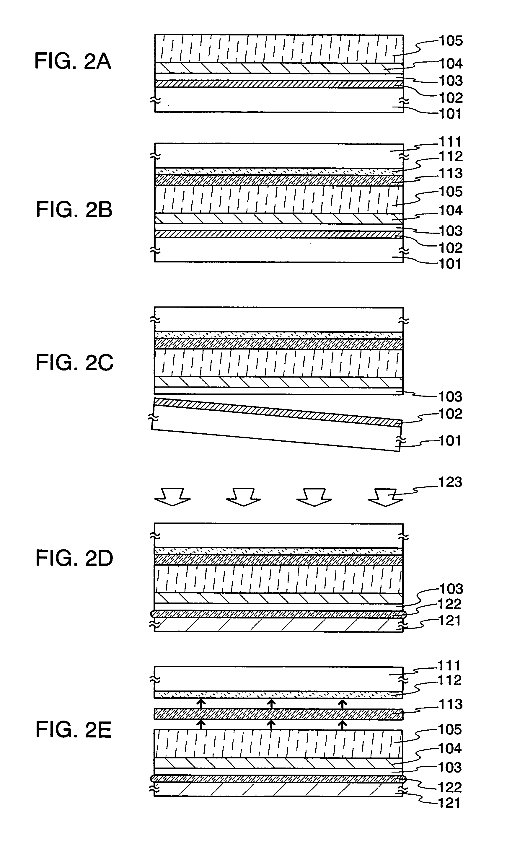
[0060] A method of manufacturing a semiconductor device using a plastic substrate as its support medium will be described in the present embodiment mode with reference to FIGS. 2A to 2E.
[0061] As shown in FIG. 2C, a metal film 102 is separated from an oxide film 103 in the same manner as the steps illustrated in FIGS. 1A to 1C in Embodiment Mode 1.
[0062] As shown in FIG. 2D, a second substrate 121 is attached to a surface of the oxide film 103, where is exposed due to the separation, by using a second adhesive material 122. As for the second adhesive material, an epoxy resin can be used. The second substrate can be made from an organic resin such as polycarbonate (PC); ARTON formed of a norbornene resin with a polar radical that is manufactured by JSR Corporation; polyethylene terephthalate (PET); polyether sulfone (PES); polyethylene naphthalate (PEN); nylon; polyether ether ketone (PEEK); polysulfone (PSF); polyetherimide (PEI); polyarylate (PAR); polybutylene terephthalate (PBT...
embodiment 1
[0066] In the present embodiment, a method of manufacturing a semiconductor device using Embodiment Mode 1 will be described with reference to FIGS. 3A to 3E and FIGS. 4A to 4D.
[0067] As shown in FIG. 3A, a metal film 302 (e.g., a tungsten film with a thickness of 10 to 200 nm, preferably, 30 to 75 nm) is formed on a first substrate 301. The metal film is heated to form an oxide film 303 (e.g., a tungsten oxide film) with a thickness of 1 to 10 nm, preferably, 2 to 5 nm.
[0068] Since the tungsten film and the tungsten oxide film are also formed on edge surfaces of the substrate by sputtering, they are preferably and selectively removed therefrom by O2 ashing etc.
[0069] An anti-reduction film 304 is formed by sputtering. In the embodiment, an AlNx Oy film is formed by using an aluminum nitride (AlN) target under an atmosphere of containing a mixture of argon gas, nitrogen gas, and oxygen gas. A first insulating film 305, e.g., a silicon oxynitride film, is next laminated by PCVD. A...
PUM
 Abstract
Description
Claims
Application Information
 - Generate Ideas
- Intellectual Property
- Life Sciences
- Materials
- Tech Scout
- Unparalleled Data Quality
- Higher Quality Content
- 60% Fewer Hallucinations
Browse by: Latest US Patents, China's latest patents, Technical Efficacy Thesaurus, Application Domain, Technology Topic, Popular Technical Reports.
© 2025 PatSnap. All rights reserved.Legal|Privacy policy|Modern Slavery Act Transparency Statement|Sitemap|About US| Contact US: help@patsnap.com