

Nanocrystal doped matrixes
- Summary
- Abstract
- Description
- Claims
- Application Information
AI Technical Summary
Benefits of technology
Problems solved by technology
Method used
Image

Examples
example 1
Core / shell Nanocrystal Synthesis
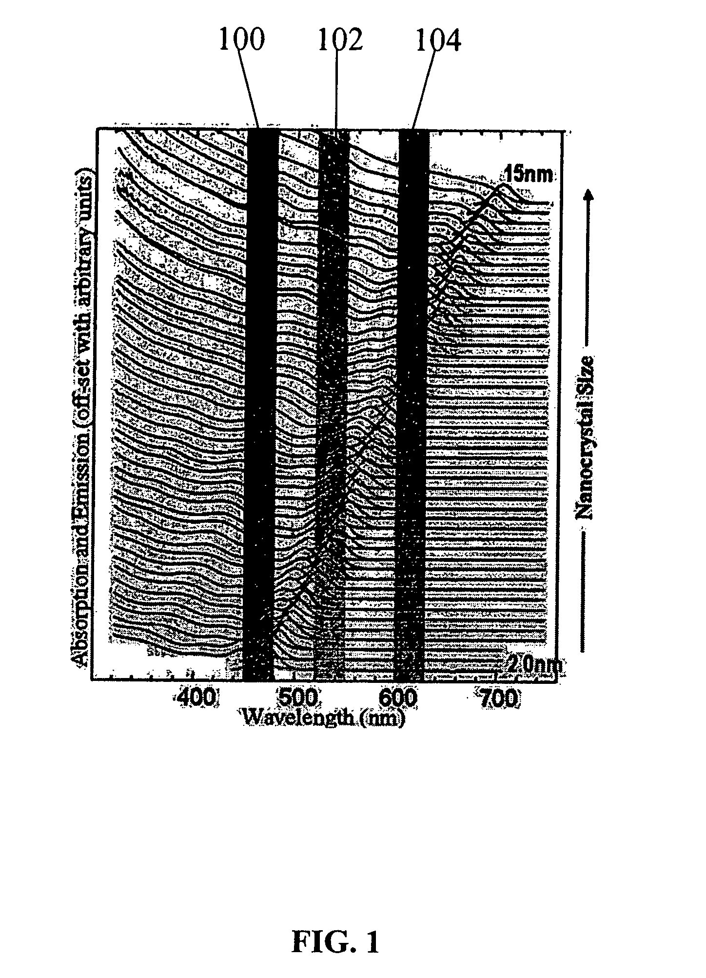
[0153] Suitable nanocrystal synthesis procedures include fabricating nanocrystal samples with specific spectral characteristics matched to those prescribed by the theoretical models of the present invention. This can include fabricating nanocrystals with tunable sizes and size distributions (e.g., sizes ranging from 1-20 nm in diameter producing emission peak wavelengths tunable between 460 and 640 nm with FWHM tunable from about 15 to about 100 nm). This in turn is used to synthesize nanocrystal mixtures identified by simulations that have the optimal emission characteristics. The simulation and core / shell nanocrystal procedure is typically performed in an iterative process.
[0154] Type I core-shell nanocrystals of CdSe / ZnS (core / shell) can be synthesized by a two step process using a solution phase method, first with the fabrication of the core material followed by growth of the shell.
Core Synthesis
[0155] Stock solutions are prepared of Se powd...
example 2
ZnS Nanocrystal Synthesis
[0160] In the order listed, add the following to a 50 mL 3-neck round bottom flask:
[0161] 1. Zn(acetate)2: 76.5 mg Lot# 12727BC
[0162] 2. Stearic Acid: 484 mg Lot# 06615MA
[0163] 3. Tri-n-octylphosphine oxide (TOPO): 4.07 g Lot# 21604LA
[0164] In a glove box prepare the following:
[0165] 3.9 g of distilled tri-n-octylphosphine (TOP) (#35-111) in 5 mL syringe;
[0166] 116.4 mg of stock solution 02-190 (bis(trimethylsilyl)sulfide (TMS2S):TOP) in 1 mL syringe; and
[0167] One 40 mL septa cap vial with 5.0 mL of MeOH
[0168] Place reactor under vacuum
[0169] Heat to 120° C.
[0170] Once at 120° C., allow to sit for 20 minutes
[0171] Place reactor under argon
[0172] Slowly inject TOP from 5 mL syringe
[0173] Change set point temperature to 250° C.
[0174] Once at 250° C., immediately inject the stock solution 02-190 (bis(trimethylsilyl)sulfide (TMS2S):TOP) from 1 mL syringe
[0175] Grow with temperature at 250° C. for 2 minutes
[0176] Remove the heating mantle and al...
example 3
Carboxylic Acid-Silicone Ligand Synthesis
[0181] General Methods
[0182] All manipulations were carried out with strict exclusion of air and moisture by using Schlenk technique under an atmosphere of dry nitrogen, unless otherwise stated. THF, toluene, chloroform-d1 and toluene-d8 were dried over activated 4 A Molecular Sieves and de-gassed by three freeze-pump-thaw cycles. 4-pentenoic acid and 1,1,1,3,5,5,5-heptamethyltrisiloxane were purchased from Aldrich (St. Louis, Mo.), distilled and stored in a storage flask using Schlenk technique before use. Heptamethyl cyclotetrasiloxane and 1,1,1,3,3,5,5-heptamethyl trisiloxane were purchased from Gelest (Morrisville, Pa.), distilled and stored in a storage flask using Schlenk technique before use. Karstedt's catalyst or platinum divinyl tetramethyl disiloxane complex, 2.1 to 2.4% in xylenes, was purchased from Gelest, stored in the glove box and used without further purification. All products were stored in the glove box. NMR chemical sh...
PUM
| Property | Measurement | Unit |
|---|---|---|
| Fraction | aaaaa | aaaaa |
| Fraction | aaaaa | aaaaa |
| Fraction | aaaaa | aaaaa |
Abstract
Description
Claims
Application Information