Methods for in-situ cleaning of semiconductor substrates and methods of semiconductor device fabrication employing the same
a technology of semiconductor substrates and cleaning methods, applied in the direction of polycrystalline material growth, dough shaping, mixing/kneading with horizontally mounted tools, etc., can solve the problems of reducing the yield of wafers, degrading the reliability of the resulting semiconductor devices, degrading electrical properties, and forming native oxides on the silicon surface, so as to reduce the likelihood of temperature-related problems and reduce the overall process time
- Summary
- Abstract
- Description
- Claims
- Application Information
AI Technical Summary
Benefits of technology
Problems solved by technology
Method used
Image
Examples
first example embodiment
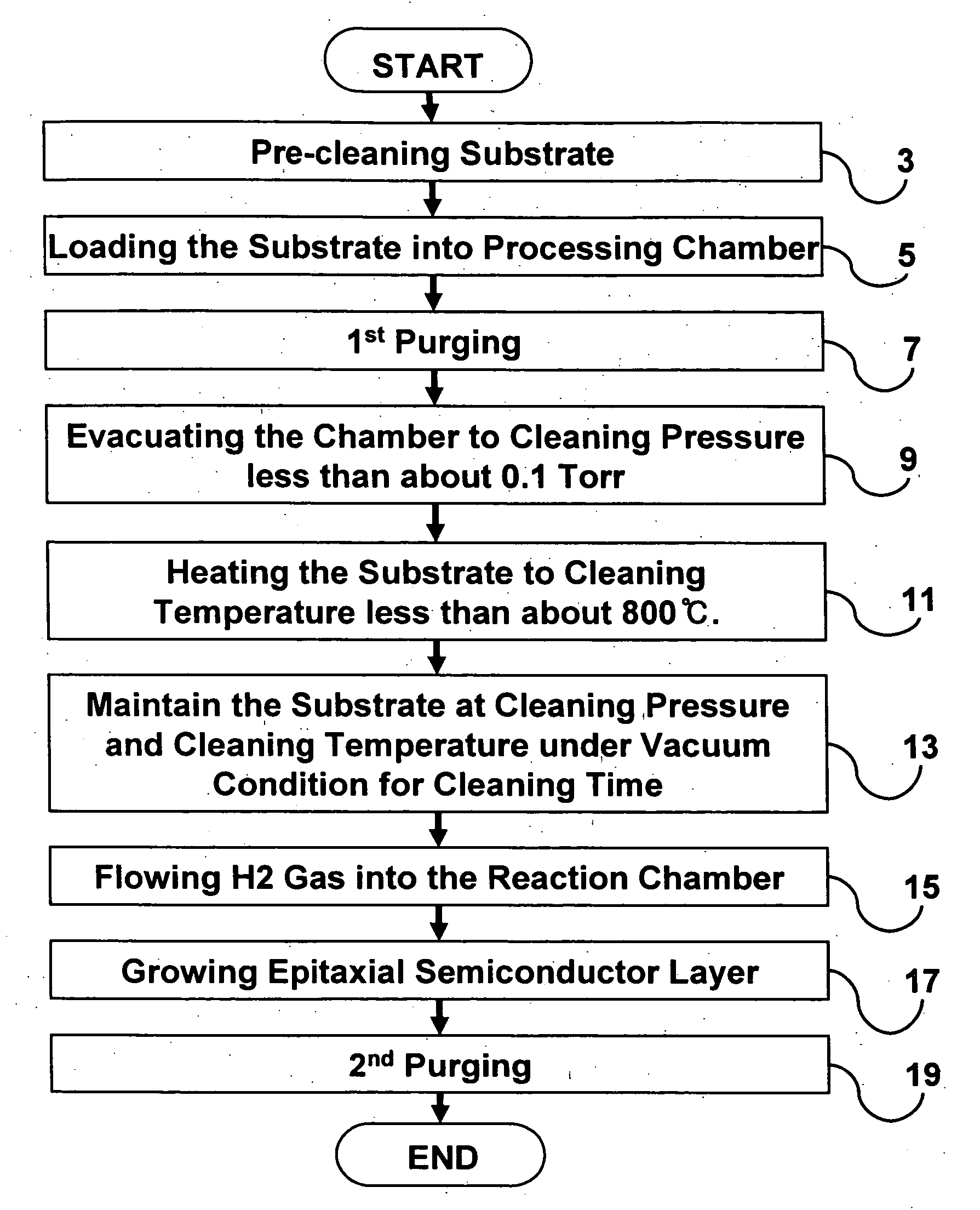
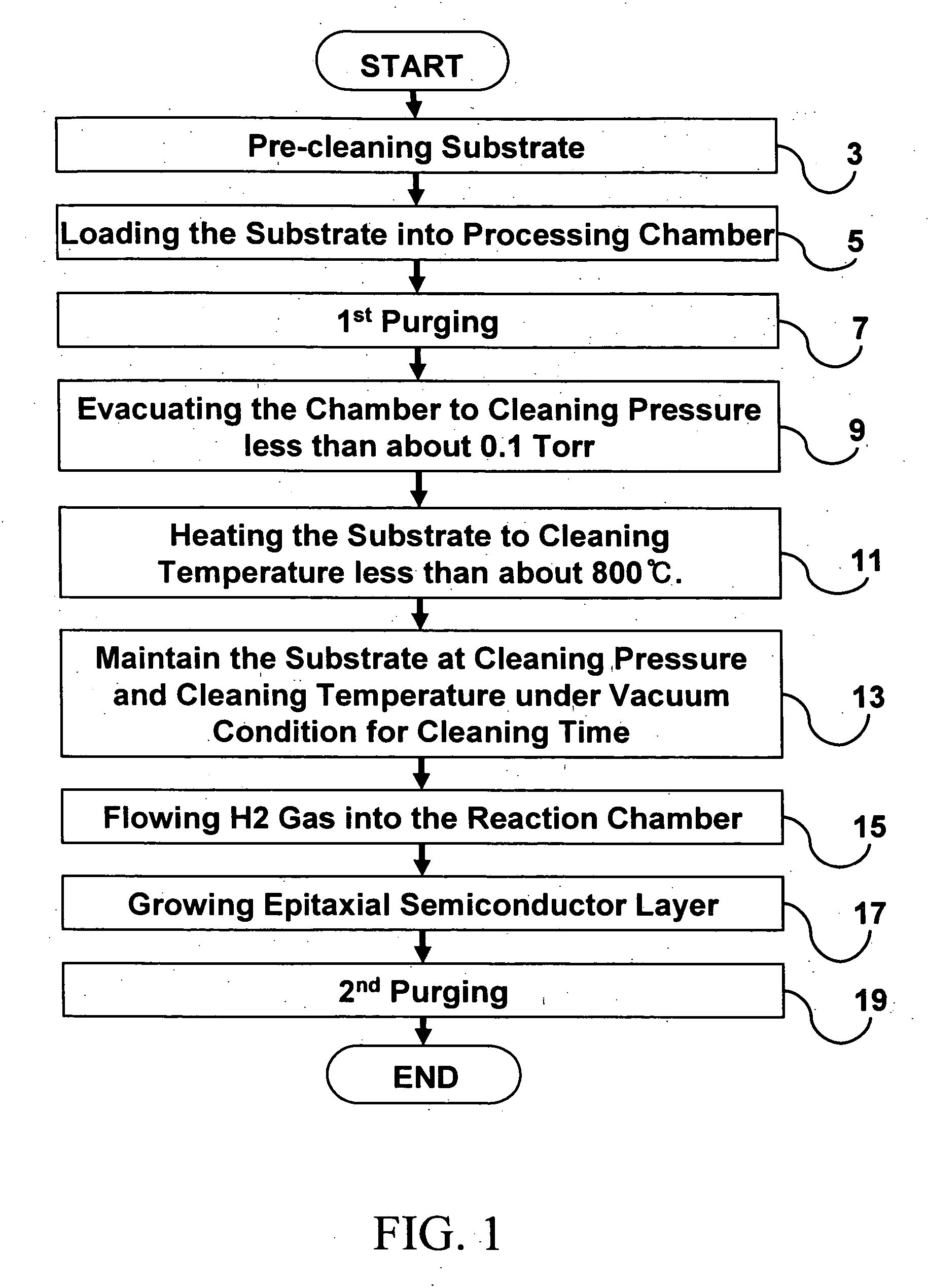
[0041] Although the examples described below will, for convenience, refer to semiconductor substrates having silicon surfaces, the invention is not so limited and may be applied to a variety of substrates including, for example, single crystal silicon substrates, silicon on insulation (SOI) substrates having single crystalline silicon, single crystal silicon-germanium substrates. Other potential substrates include single crystal germanium substrates and single crystal silicon-carbide substrates as well as a variety of tertiary and quaternary semiconductors including, for example III-IV and II-V semiconductor compounds such as AlxInyGa1-xN and other semiconductor compounds known to those of ordinary skill in the art.
[0042] The cleaning methods according to the invention may be utilized with both unprocessed substrates and processed substrates that have already completed a substantial portion of the fabrication process. The processed substrates may already include a variety of circui...
second example embodiment
[0059] An example embodiment of a semiconductor fabrication process is illustrated in FIGS. 3A-3D. As illustrated in FIG. 3A, a semiconductor substrate 100, typically comprising silicon, silicon / germanium, silicon carbide or germanium, is processed to form shallow trench isolation (STI) structures 102, thereby defining active regions on the surface of the semiconductor substrate. A gate structure or pattern 110 is then formed in the active region. The gate structure 110 will typically include a dielectric or gate oxide layer 104 formed directly on the surface of the substrate, a gate electrode 106, typically a doped polysilicon or amorphous silicon layer arid, in some instances, silicide or salicide layers (not shown) for reducing the resistance of the gate electrode, and, optionally, a capping layer 108, for example silicon nitride, for protecting at least the upper surface of the gate electrode.
[0060] As illustrated in FIG. 3B, the gate structure 110 may be used as an implant mas...
PUM
| Property | Measurement | Unit |
|---|---|---|
| temperature | aaaaa | aaaaa |
| pressure | aaaaa | aaaaa |
| temperature | aaaaa | aaaaa |
Abstract
Description
Claims
Application Information


