Copper alloy and liquid-crystal display device

a display device and copper alloy technology, applied in the direction of instruments, solid-state diffusion coatings, coatings, etc., can solve the problems of insufficient electronegativity described in the patent document 1, inability to prevent oxidation, and inability to form oxide films having high adhesion to the cu surface, etc., to achieve the effect of easy formation

Active Publication Date: 2007-01-04
XENOGENIC DEV LLC
View PDF7 Cites 44 Cited by
  • Summary
  • Abstract
  • Description
  • Claims
  • Application Information

AI Technical Summary

Benefits of technology

[0031] In the liquid crystal display device, an oxide film can be easily forme

Problems solved by technology

Cu is similar to Fe, and a Cu oxide is permeable to oxygen, and hence has no ability to prevent oxidation and cannot serve as a protective film.
However, the electronegativity described in the Patent document 1 is not sufficient to form an oxide film having high adhesion to the Cu surface.
In addition to the reports on the copper alloy containing Mg, there are reports on the formation of protective films from alloys containing Al or Ti, but these alloying elements have a drawback in that they increase the electric resistance of Cu.
The Patent document 3 has a problem in that titanium remains as a solid solution element or forms an inter-metallic compound to increase the electric resistance.
In the Patent document 4, a copper compound having such a high corrosion resistance that the relative oxidation number is equal to or less than 50% of that of copper is formed on the surface of copper, which poses a problem in that the productivity is low due to the formation of a compound.
The Nonpatent literature 1 has a problem in that both the Cu—Mg alloy and Cu—Al alloy subjected to heat treatment are increased in electric resistance.
Recently, in substrates having mounted electronic parts, such as a resistance, a capacitor, and a quartz clock, semiconductor elements, such as a TFT, a CMOS, and an FRAM, and semiconductor devices having mounted them, examples of wiring materials conventionally used include high melting-point metals, such as Mo and Cr, but these metals have a problem in that they have low conductivity.
However, Al poses problems of the formation of Hillocks and the occurrence of electromigration.
Al—Nd has an electric resistance lower than that of Cr; however, Al and Nd do not form solid solution, making it difficult to produce a sputter target.
Further, the Al—Nd alloy contains Nd, which disadvantageou

Method used


Image

  • Copper alloy and liquid-crystal display device
  • Copper alloy and liquid-crystal display device
  • Copper alloy and liquid-crystal display device

Examples


example

First Embodiment

[0073] The above embodiment is explained in further detail below.

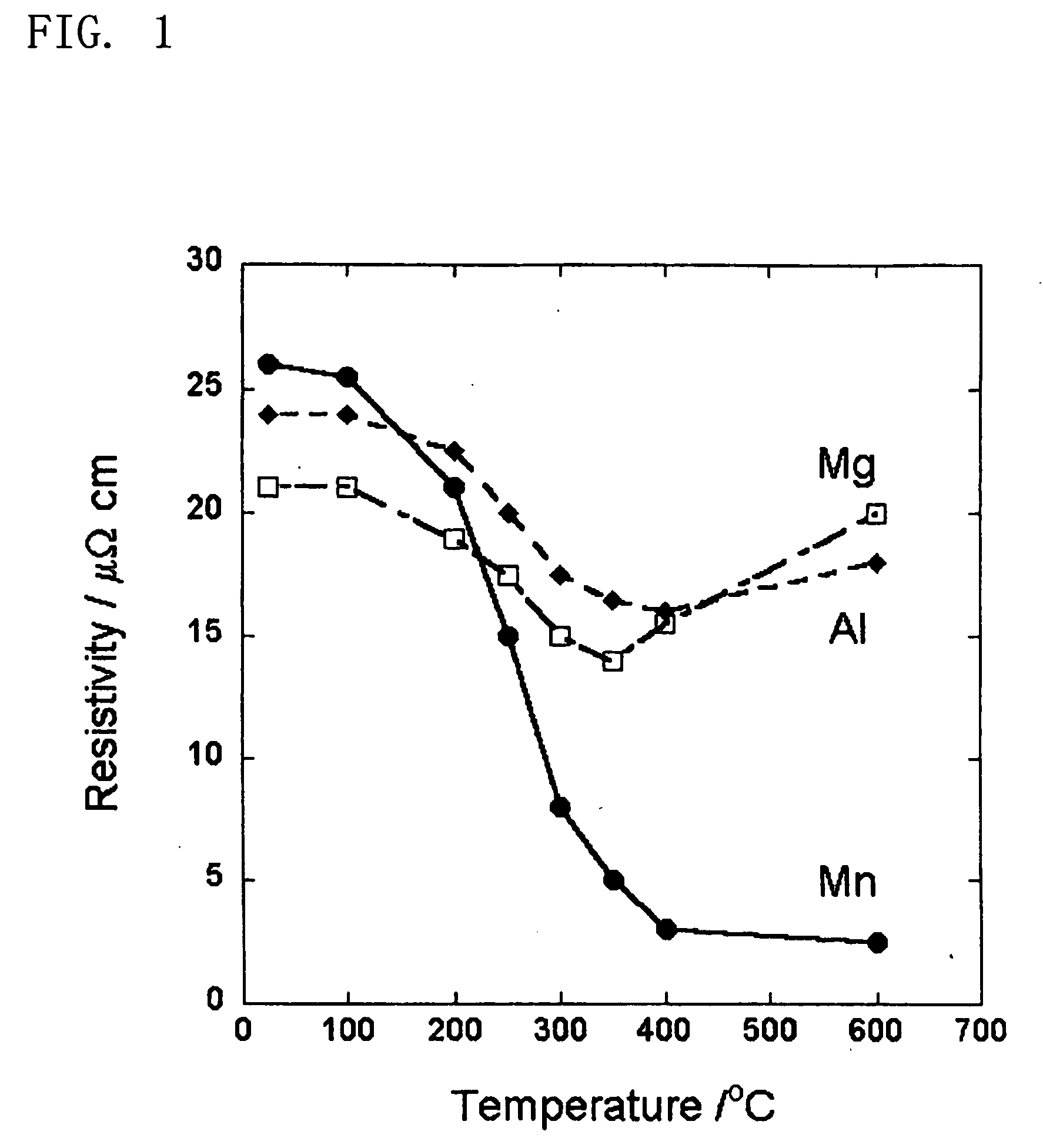
[0074] Using a Cu—Mn alloy of Cu having a purity of 99.9999% and Mn having a purity 99.98% as a sputtering target material, a Cu-7 at. % Mn alloy thin film was formed on an Si substrate having SiO2 on its surface. The resultant alloy thin film was subjected to heat treatment in an Ar gas atmosphere (oxygen content: 100 ppm) at 400° C. for 30 minutes. Element concentration distribution in the thicknesswise direction of a specimen from the surface was then determined using secondary ion mass spectrometry (SIMS).

[0075]FIG. 5 shows results of the concentration distribution determined by the SIMS. A specimen was scraped by an ion beam in the direction from the surface of the thin film to SiO2 and mass of secondary ions being sputtered from the specimen was continuously measured to determine the concentration distribution inside the specimen. It has been found that MnOx is present on the surface. The prese...

second embodiment

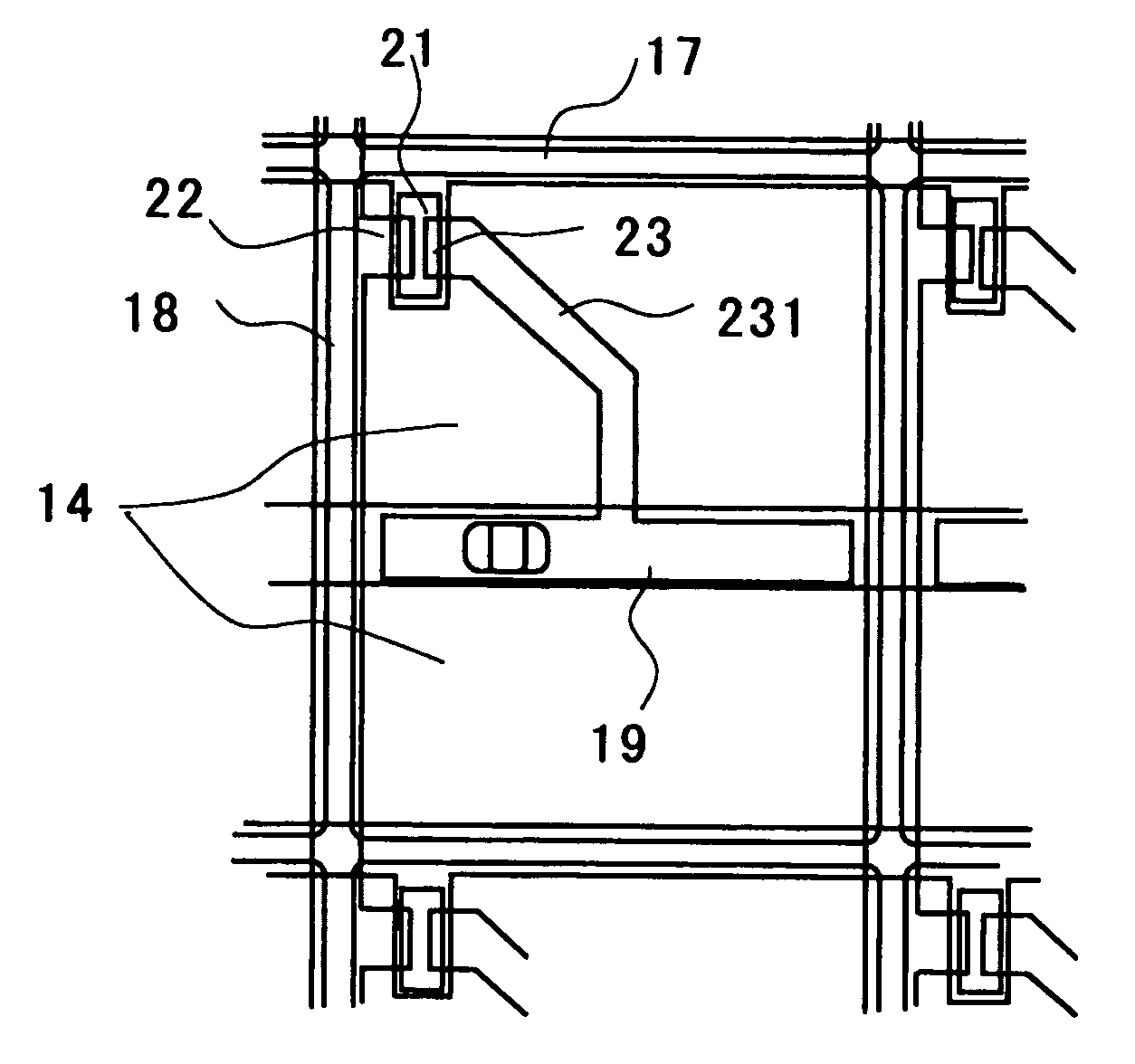
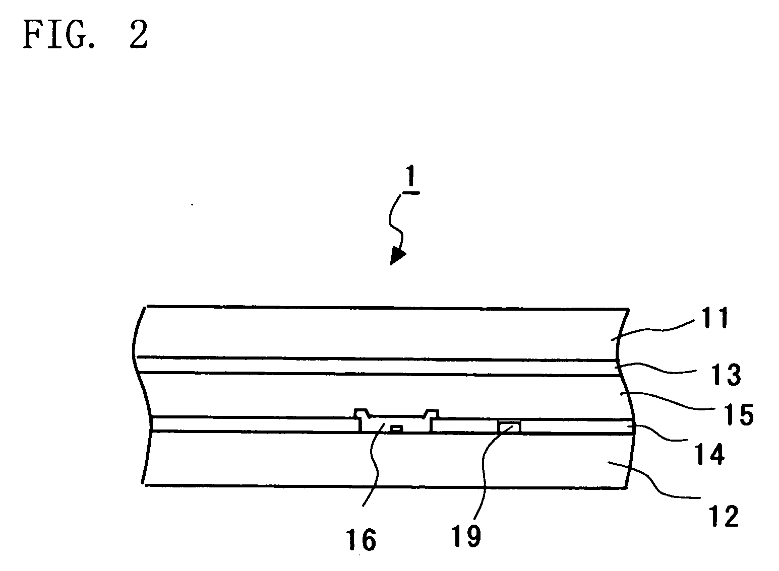
[0078] In a channel etched amorphous silicon (a-Si) TFT liquid crystal display device, the gate wiring shown in FIG. 2 is formed as follows. A Cu-2 at. % Mn alloy thin film is first formed on a washed glass substrate using a Cu-2 at. % Mn alloy of Cu having a purity of 99.9999% and Mn having a purity of 99.98% as a target material. A wiring pattern for gate line is formed on the resultant alloy thin film by a photoresist process and a dry etching process. The pattern is then subjected to heat treatment in an Ar gas atmosphere (oxygen content: 100 ppm) at 400° C. for 30 minutes. Stable oxide layers are formed at the interface between the Cu—Mn alloy and the glass substrate and on the surface of the Cu—Mn alloy.

third embodiment

[0079] A planar polysilicon (p-Si) TFT liquid crystal display device is produced as follows. A p-Si film is first deposited on a washed glass substrate by a plasma enhanced chemical vapor deposition (PECVD) process, and then thoroughly subjected to laser annealing. The p-Si film is patterned and then an SiO2 gate insulator film is formed by a CVD process. A film of a Cu-2 at. % Mn alloy is then formed by a sputtering process and etched to form a gate electrode. Next, the resultant substrate is subjected to heat treatment in a vacuum at 400° C. for 30 minutes. The substrate is subsequently doped with an impurity by an ion doping process, and a source and a drain are formed in a self-alignment manner, forming an interlayer dielectric film. The resultant substrate is then subjected to heat treatment at 400° C. for 30 minutes. FIG. 8 is a schematic diagram of thus formed planar polysilicon (p-Si) TFT through the above steps. In FIG. 8, an oxide comprised of Mn is formed on the gate insu...


PUM

PropertyMeasurementUnit
Temperatureaaaaaaaaaa
Timeaaaaaaaaaa

Abstract

To provide a highly conductive Cu alloy which is advantageous in that an alloying element added to Cu is first reacted with oxygen contained in a gas atmosphere or solid in contact with the Cu member to form an oxide film which can prevent oxidation of Cu. The copper alloy comprises copper (Cu) containing an inevitable impurity, and an element added to the copper, wherein the added element is capable of being dissolved in the copper in an amount of 0.1 to 20 at. %, wherein the added element has an oxide formation free energy smaller than that of Cu and has a diffusion coefficient in Cu larger than the self-diffusion coefficient of Cu.

Description

BACKGROUND OF THE INVENTION [0001] 1) Field of the Invention [0002] The invention relates to a copper alloy which has a low electric resistance, and can easily form a stable oxide film layer on its surface and its interface, and a liquid crystal display device using the copper alloy in wirings. [0003] 2) Description of the Related Art [0004] While many metals suffer oxidation on their surfaces and hence deteriorate in performance, aluminum (Al) and alloys thereof form an Al oxide on their surfaces, and the Al oxide serves as a protective film which can prevent oxidation on the surface. With respect to iron (Fe), Fe itself does not form a protective film, but, in the form of stainless steel which is an Fe alloy containing chromium (Cr), Cr in stainless steel forms a protective film, which can prevent oxidation on the surface. [0005] Cu is similar to Fe, and a Cu oxide is permeable to oxygen, and hence has no ability to prevent oxidation and cannot serve as a protective film. When an ...

Claims


Application Information

Patent Timeline
IPC IPC(8): G02F1/1343
CPCC22C9/05C23C8/10G02F1/136286G02F1/1368G02F2001/136295H01L27/124H01L21/76852H01L21/76867H01L29/458H01L29/4908H01L21/76834G02F1/136295
Inventor KOIKE, JUNICHI
Owner XENOGENIC DEV LLC
Why Eureka
Try Eureka