

Low-Doped Semi-Insulating Sic Crystals and Method
- Summary
- Abstract
- Description
- Claims
- Application Information
AI Technical Summary
Benefits of technology
Problems solved by technology
Method used
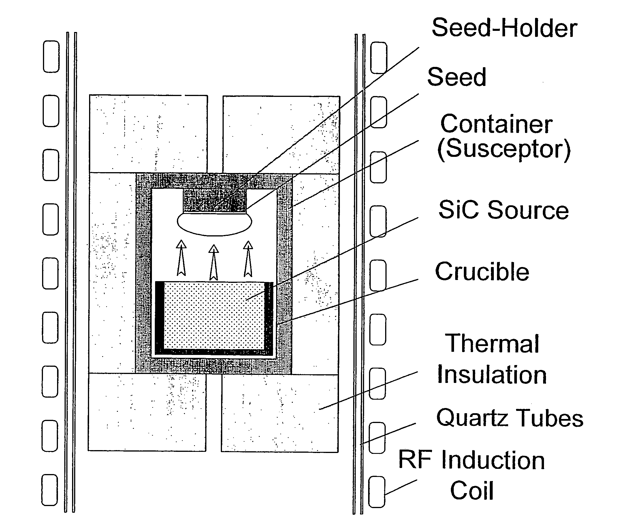
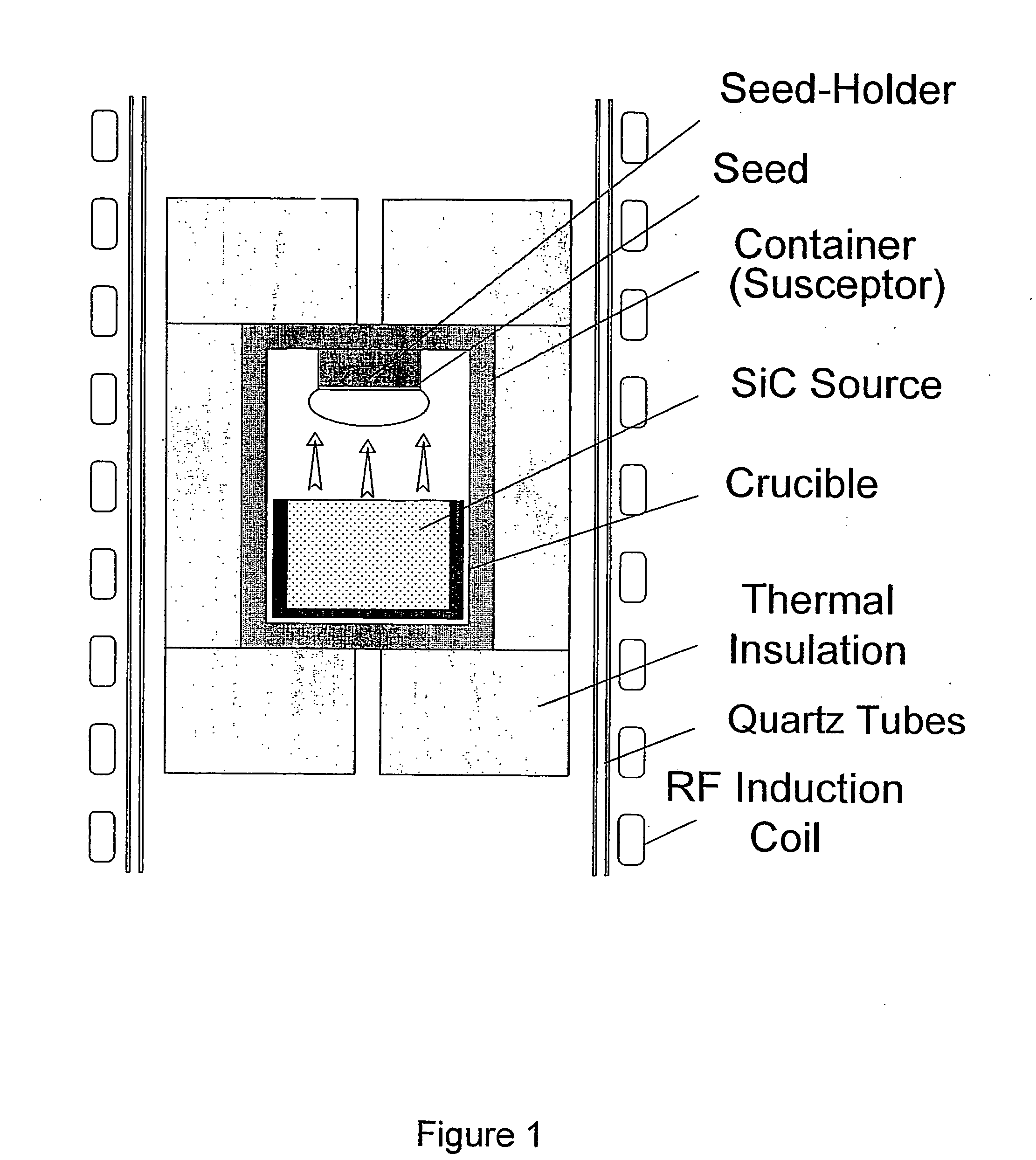
Image

Examples
example 1
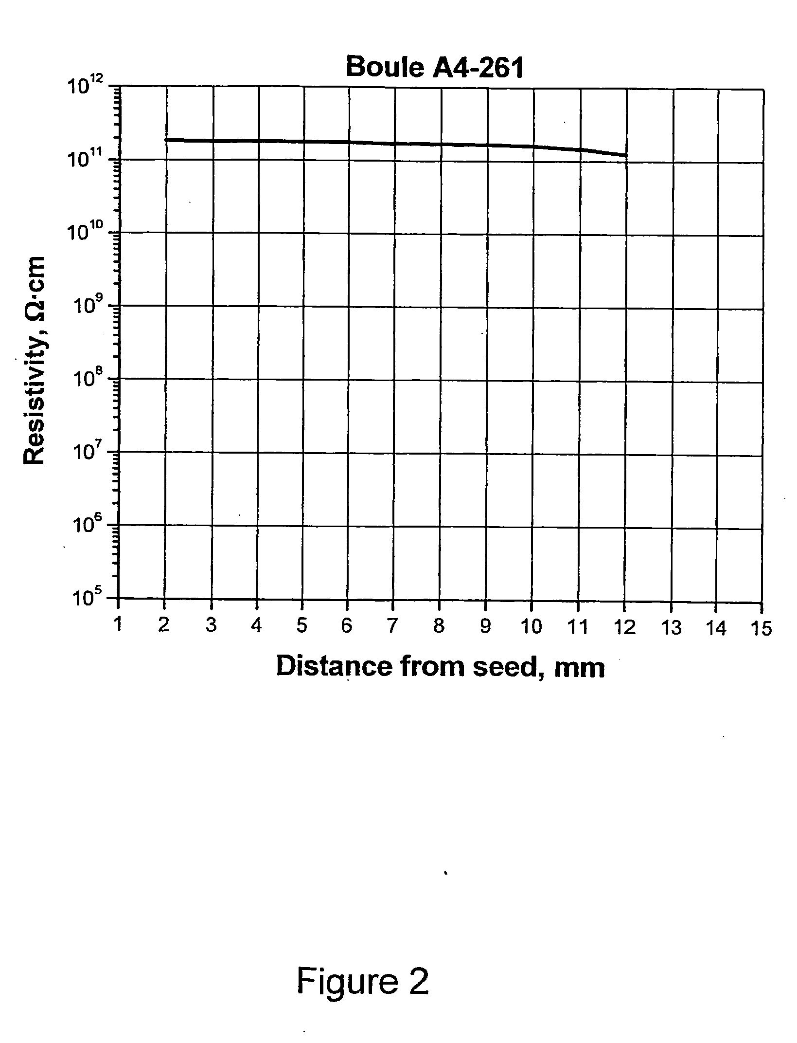
[0049]A 2-inch diameter vanadium-doped semi-insulating SiC crystal (boule A4-261) was grown at a seed temperature of 2050° C. and source temperature of 2100° C. The growth ambient was 10 torr of helium. The resulting crystal exhibited a very high and uniform resistivity above 1011 Ohm-cm, as illustrated in FIG. 2, with the standard deviation in resistivity across the substrate areas of about 3.5%. The substrate capacitance measured by a mercury probe at 10 kHz was below 0.2 pF / mm2.
[0050]The impurity content of crystal A4-261 was analyzed using Secondary Ion Mass Spectroscopy (SIMS). The results are shown in Table 3.
TABLE 3Impurity content in SI SiC crystal A4-261, cm−3.BNVAlTi2.3 · 10164.9 · 10166.0 · 10163.0 · 10144.0 · 1014
[0051]The vanadium content is nearly an order of magnitude lower than its solubility in SiC, but at the same time it is roughly two times higher than the net shallow impurity concentration (nitrogen minus boron). In this case, the nitrogen concentration was high...
example 2
[0053]A 2-inch diameter vanadium-doped semi-insulating SiC crystal (boule A1-367) was grown in conditions similar to those of Example 1 (boule A4-261), except special measures were taken during growth in order to minimize the content of residual nitrogen in the crystal and make it below that of boron.
[0054]The impurity content of boule A4-367 has been analyzed using SIMS, and the results are shown in Table 4.
TABLE 4Impurity content in SI SiC crystal Al-367, cm−3.BNVAlTi4.3 · 10169 · 10155.3 · 10163.0 · 10142.0 · 1014
[0055]The SIMS data demonstrates the nitrogen content is reduced to a level below that of boron. One can also see that, similar to Example 1, the vanadium content is substantially lower than its solubility limit and it is sufficiently higher than the net shallow impurity concentration (boron minus nitrogen) to achieve semi-insulating behavior, as described below.
[0056]A combination of sufficient vanadium doping with a relatively low level of nitrogen resulted in an extre...
example 3
[0057]A 2-inch diameter vanadium-doped semi-insulating SiC crystal (boule A4-270) was grown in conditions similar to those described above. Similar to Example 2, special measures were taken during growth to minimize the nitrogen background contamination.
[0058]The axial distribution of resistivity in boule A4-270 shown in FIG. 3 demonstrates a very high and uniform resistivity, close to 3·1011 Ohm-cm. The substrate capacitance was below 0.1 pF / mm2.
[0059]The impurity content of crystal A4-270 is shown in Table 5.
TABLE 5Impurity content in SI SiC crystal A4-270, cm−3.BNVAlTi1.15 · 10168.1 · 10153.53 · 10163.0 · 10141.0 · 1014
[0060]The SIMS data demonstrates a level of nitrogen below that of boron and the vanadium concentration about four times higher than the net shallow impurity concentration (boron minus nitrogen). No vanadium precipitates or any other vanadium-related defects were present in the boule.
PUM
 Abstract
Description
Claims
Application Information