

Low resistivity single crystal silicon carbide wafer
a technology of silicon carbide and single crystal, which is applied in the direction of after-treatment details, instruments, transportation and packaging, etc., can solve the problems of many stacking faults and the inability to ignore the wafer resistance of the single crystal wafer, and achieve excellent electrical properties, low resistance, and low resistance
- Summary
- Abstract
- Description
- Claims
- Application Information
AI Technical Summary
Benefits of technology
Problems solved by technology
Method used
Image


Examples
example 1
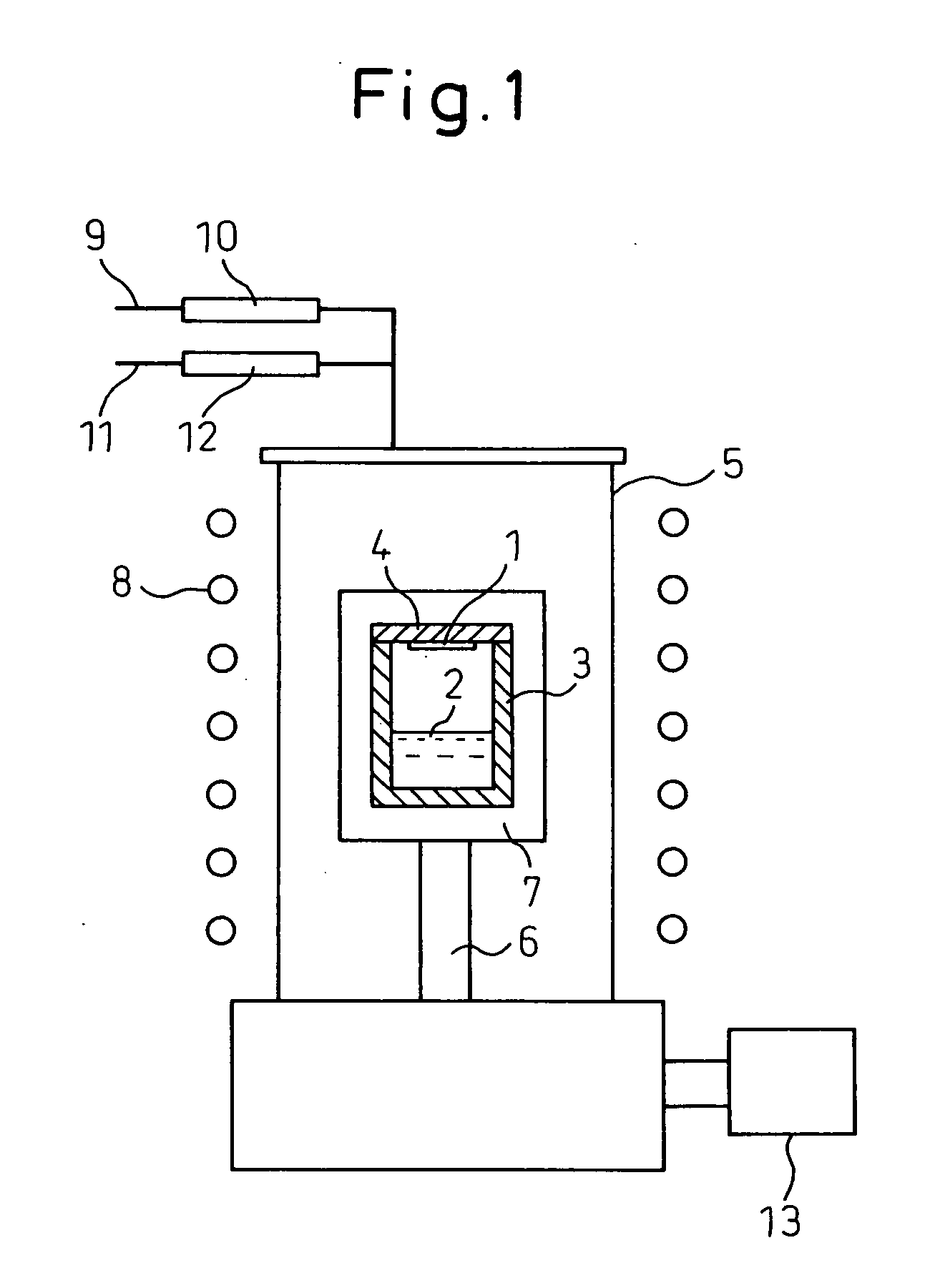
[0057]FIG. 1 is an example of an SiC single-crystal growth apparatus utilizing the modified Lely process, which is used to produce the low resistivity SiC single crystal wafer according to the present invention. The single-crystal growth apparatus will be briefly explained first. Crystal growth is conducted by subliming SiC powder 2 (feedstock) and recrystallizing the sublimed SiC on SiC single-crystal 1 used as seed crystal. The SiC single crystal 1 that is the seed crystal is attached to the inner surface of a graphite lid 4 of a graphite crucible 3. The feedstock SiC powder 2 is charged into the graphite crucible 3. The crucible 3 is mounted on a graphite support rod 6 inside a double-wall quartz tube 5. Graphite felt 7 is installed around the graphite crucible 3 to form a heat shield. The double-wall quartz tube 5 can be evacuated to a high vacuum (10−3 Pa or less) by a vacuum pumping apparatus 13. The pressure of the internal atmosphere is controlled with argon gas and nitrogen...
example 2
[0071]In order to examine the effect of wafer surface roughness, an experiment was conducted using a different polishing method from that in Example 1. A low resistivity SiC single crystal ingot was grown as in Example 1. A wafer cut from the ingot to the same specifications (plane orientation and thickness) as in Example 1 was polished using a diamond slurry of 0.5 μm grain size. The polished wafer thickness was 0.35 mm and its average surface roughness (Ra) was 0.6 nm. Both sides of the wafer were polished, so that 95% or greater of the entire surface area was covered by a smooth surface of a roughness of 1.0 nm or less.
[0072]The wafer fabricated was then annealed for 2 h at 1100° C. in an argon atmosphere. The average stacking fault density of the annealed wafer determined by molten KOH etching was 21 cm−1. The average stacking fault density was substantially the same in the case of other wafers subjected to similar high-temperature annealing at 1200° C. and 1400° C.
example 3
[0073]In order to examine the effect of wafer resistivity, an experiment was conducted similarly to in Example 1 but using a wafer of different resistivity.
[0074]As in Example 1, SiC single crystal was produced by the modified Lely process. The crystal growth was conducted in an atmosphere gas of argon gas containing 33% nitrogen gas. A wafer of 50.8-mm diameter and 0.4-mm thickness was cut from the grown SiC single crystal ingot to have a plane offset from {0001} of 8° toward [11-20]. The wafer was mechanochemically polished using a colloidal silica slurry containing an oxidation accelerator (aqueous hydrogen peroxide solution). The polished wafer thickness was 0.35 mm. Both sides of the wafer were polished, so that 95% or greater of the entire surface area was covered by a smooth surface of a roughness of 0.22 nm or less. When the resistivity of the wafer was measured by the eddy current method, the value obtained was 0.0114 Ωcm.
[0075]The wafer was then placed in a high-temperatur...
PUM
 Abstract
Description
Claims
Application Information