Method for the fabrication of periodic structures on polymers using plasma processes

a technology of periodic structure and plasma process, which is applied in the field of plasma-directed method of self-assembly of polymer, can solve the problems of affecting the optical properties, affecting the surface, and exhibiting a peaked fft, etc., and achieves enhanced anti-reflective performance, affecting optical properties, and enhancing anti-reflective performance.

Inactive Publication Date: 2011-07-07
GOGOLIDES EVANGELOS +7
View PDF8 Cites 20 Cited by
  • Summary
  • Abstract
  • Description
  • Claims
  • Application Information

AI Technical Summary

Benefits of technology

[0035]Such highly periodic controlled AR structures are also shown to be valuable to control the reflectivity of surfaces and to tune it to the appropriate broadband or peaked reflector. Accordingly, in a related embodiment, the invention provides a method for the fabrication of nanostructures on polymeric surfaces by means of plasma processing and wherein the resulting polymeric surfaces have enhanced antireflective performance, which method comprises providing a polymeric surface comprising nanostructures and fabricated in accordance with any of the methods of the main aspect of the invention, wherein, during the plasma treatment step of any of the methods of the main aspect, fast etching plasmas are utilised with ions having energy less than or equal to 100 eV. In acco

Problems solved by technology

Self-assembly methods (as defined below) often lead to surfaces exhibiting a peaked FFT, and several oscillations in the HHCF.
However conventional photolithography schemes, although capable of achieving below 32 nm resolution using 193 nm lithography and resolution enhancement methods, or Extreme Ultra Violet Lithography (EUV) at 13.5 nm, are extremely costly.
Other “top down” methods such as electron beam or ion beam lithography are slow step-wise processes.
Definitions of “self-assembly” vary hugely and generalisation is somewhat difficult1.
The self-assembly processes, however, suffer from a poor degree of control of spatial and size distribution of the resulting nanostructures.
Furthermore, the processes are only applicable to limited classes of materials.
Additionally, there are often problems with low throughput or low homogeneity in large areas of the pattern.
Moreover, by-products are sometimes generated in the wet-chemical preparation, which makes it difficult to keep the surface clean.
Since, among other drawbacks, periodicity cannot be controlled over large area

Method used


Image

  • Method for the fabrication of periodic structures on polymers using plasma processes
  • Method for the fabrication of periodic structures on polymers using plasma processes
  • Method for the fabrication of periodic structures on polymers using plasma processes

Examples


example 1

Highly Periodic Pattern Formation on PMMA Plates by Oxygen Plasma Treatment at 0 V Bias

[0058]PMMA in a 2 mm thick sheet-form (purchased from IRPEN, Spain) is used as delivered (with only a few seconds cleaning with isopropanol) with no other special pre-treatment. A plasma reactor (MET-Alcatel), equipped with a helicon source (at 13.56 MHz), providing RF top-power 2000 W is used, to provide high neutral and ion flux. The electrode is not externally biased, and is set at 50° C. The chamber is fed with 100 sccm O2 and set at 0.75 Pa. The chamber walls are made of Anodized Al, and the plasma source wall from Al2O3. It is clarified that this particular reactor does not have an electrostatic shield for the RF fields of the helicon source antenna, and as a result source wall material is sputtered due to high capacitive voltages developing in the source.

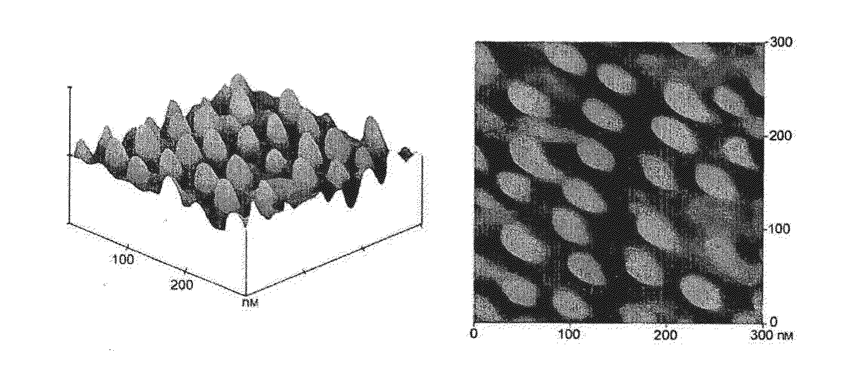
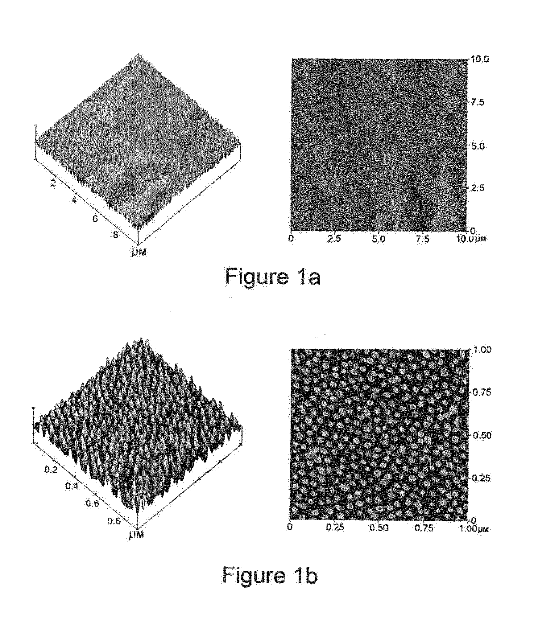
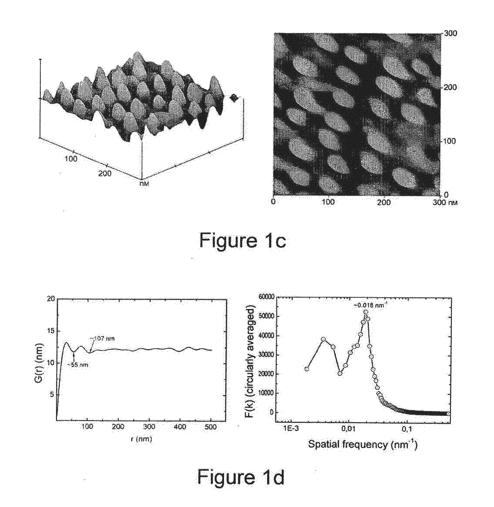
[0059]FIG. 1 demonstrates three different magnification Atomic Force Microscopy (AFM) images of the same PMMA sheet surface after 5 min Ox...

example 2

Effect of Processing Time on Geometrical Characteristics of Highly-Periodic Patterns

[0060]PMMA plates were treated as described in example 1 for 3 and 5 min. Scaling analysis showed the following results:

RMSAverage widthAverage spacingConditionsin nm(2 ·ξ) in nmin nm, wavelength 3 min, 50° C.4.91627.5 5 min, 50° C.8.6285515 min, 50° C.25

[0061]As time proceeds the periodic mounds grow higher, wider, and with a larger spacing. The periodicity persists for several minutes of processing, but is lost at long processing times (15 min in this example).

example 3

Effect of Sample Temperature on Geometrical Characteristics of Highly-Periodic Patterns

[0062]PMMA samples were treated as described in example 1, but the temperature was kept higher 75° C. Scaling analysis results are shown below and compared with example 1.

RMSAverage widthAverage spacingConditionsin nm(2 ·ξ) in nmin nm, wavelength3 min, 50° C.4.91627.55 min, 75° C.10.2362116

[0063]As can be seen, increasing the temperature the height, width, and spacing between nanostructures are increased.


PUM

PropertyMeasurementUnit
Temperatureaaaaaaaaaa

Abstract

This invention presents a method for the fabrication of periodic nanostructures on polymeric surfaces by means of plasma processing, which method comprises the following steps:
  • (i) provision of a homogeneous organic polymer (such as PMMA, or PET, or PEEK, or PS, or PE, or COC) or inorganic polymer (such as PDMS or ORMOCER);
  • (ii) exposure of the polymer to an etching plasma such as oxygen (O2) or sulphur hexafluoride (SF6) or a mixture of oxygen (O2) and sulphur hexafluoride (SF6), or mixtures of etching gases with inert gases such as any Noble gas (Ar, He, Ne, Xe).

Description

FIELD OF THE INVENTION[0001]This invention relates to a plasma-directed method of self-assembly for the fabrication of periodic structures with controlled geometrical characteristics on polymer / plastic materials. These have applications in nano-patterning for nanoelectronics, nanophotonics and related fields.BACKGROUND TO THE INVENTION[0002]Periodic and well-defined features in the nano-scale are essential in several fields. These include photonics, optical applications such as diffraction gratings and antireflection surfaces, nanoelectronics, high-density information storage media, catalysis, bioanalytics, medicine and many others.[0003]The “periodicity” of a pattern formed on a surface can be mathematically rigorously described by performing a circularly averaged Fast Fourier Transform (FFT) of the surface heights, or by calculating the Height-Height Correlation Function (HHCF) of a surface. A completely periodic, deterministic surface will display an approximately delta-function ...

Claims


Application Information

Patent Timeline
IPC IPC(8): B32B3/30C23F1/00B29D99/00C23F1/04B29D11/00B82Y20/00B82Y30/00B82Y40/00
CPCB29C59/14B29K2023/06B29K2025/00Y10T428/24479B29K2067/00B29K2083/00B29K2033/12
Inventor GOGOLIDES, EVANGELOSTSEREPI, AAGELIKECONSTANTOUDIS, VASSILIOSVOURDAS, NIKOLAOSBOULOUSIS, GEORGIOSVLACHOPOULOU LACHOPOULOU, MARIA-ELENMATSOUGENI, AIKATERINIKONTZIAMPASIS, DIMITRIOS
Owner GOGOLIDES EVANGELOS
Why Eureka
Try Eureka