

Method for manufacturing soi substrate
- Summary
- Abstract
- Description
- Claims
- Application Information
AI Technical Summary
Benefits of technology
Problems solved by technology
Method used
Image

Examples
embodiment 1
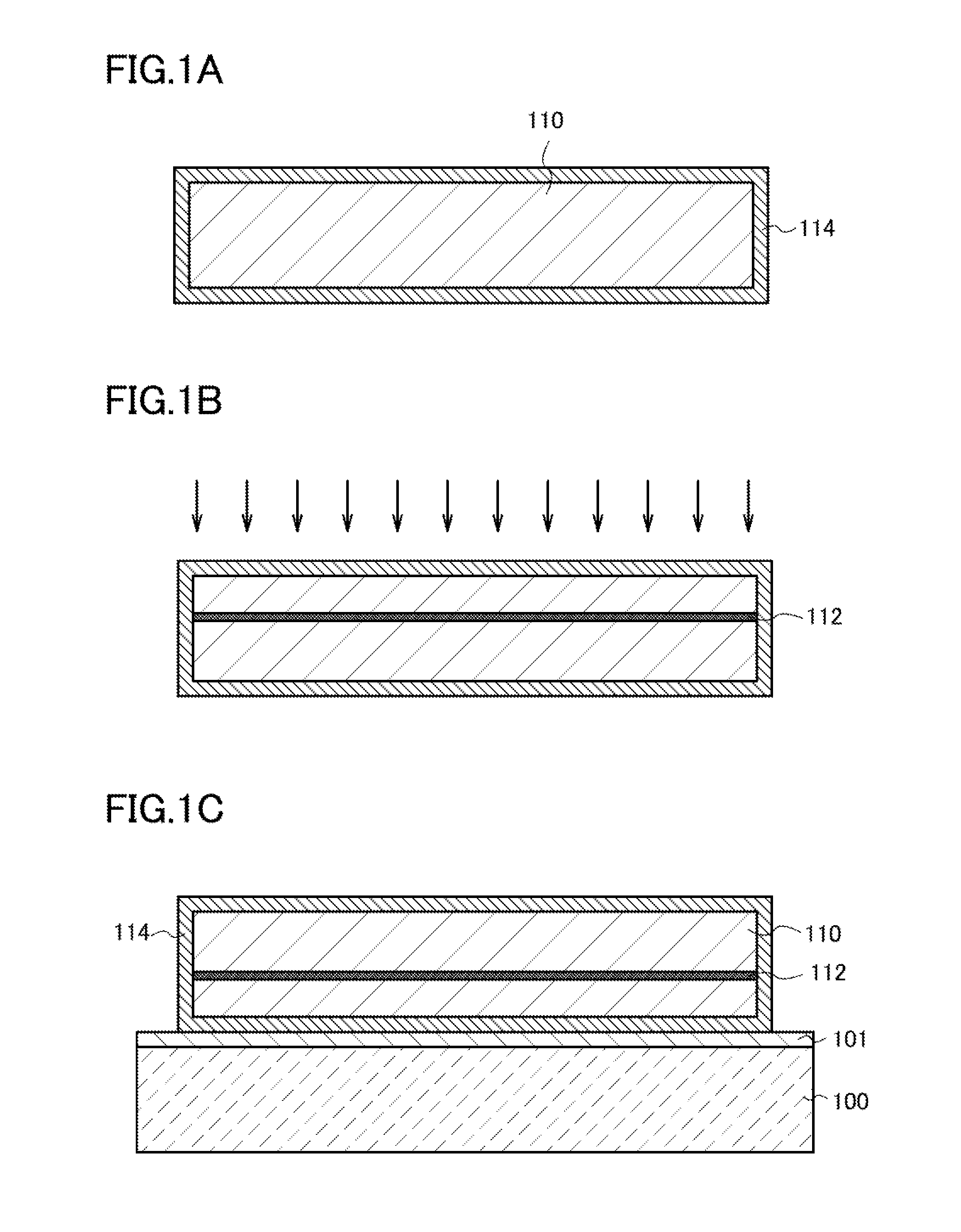
[0038]First, as a bond substrate, a semiconductor substrate 110 is prepared. As the semiconductor substrate 110, a polycrystalline semiconductor substrate or a single crystal semiconductor substrate can be used. As the semiconductor substrate 110, for example, a semiconductor substrate that is formed using an element which belongs to Group 14, such as a polycrystalline or single crystal silicon substrate, a polycrystalline or single germanium substrate, a polycrystalline or single silicon germanium substrate, or a polycrystalline or single silicon carbide substrate, or a polycrystalline or single compound semiconductor substrate using gallium arsenide, indium phosphide, or the like can be given. A typical silicon substrate is a circular substrate having a size of 5 inches (125 mm) in diameter, 6 inches (150 mm) in diameter, 8 inches (200 mm) in diameter, and 12 inches (300 mm) in diameter. Note that the shape of a silicon substrate is not limited to the circular shape, and a silicon...
embodiment 2
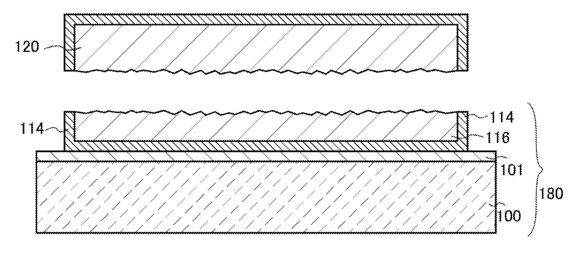
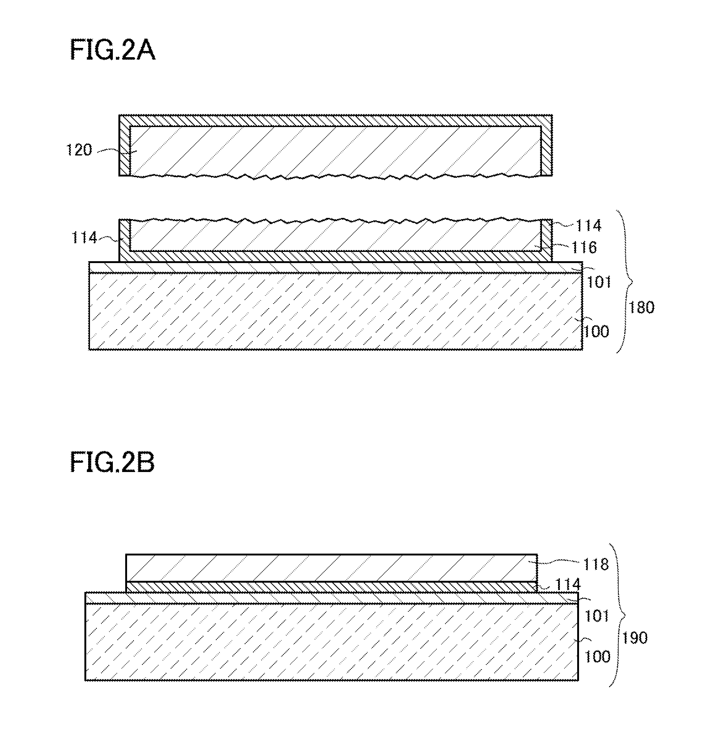
[0087]FIG. 6A is a cross-sectional view illustrating part of the SOI substrate (see FIG. 2B) manufactured with the method described in Embodiment 1.
[0088]In order to control the threshold voltage of a thin film transistor (TFT), a p-type impurity element such as boron, aluminum, or gallium, or an n-type impurity element such as phosphorus or arsenic may be added to the semiconductor layer 118. A region to which the impurity element is added and the kind of impurity element to be added can be changed as appropriate. For example, a p-type impurity element is added to a formation region of an n-channel TFT, and an n-type impurity element is added to a formation region of a p-channel TFT. The above impurity element may be added at a dose greater than or equal to 1×10¹¹ ions / cm2 to 1×10¹⁴ ions / cm2.
[0089]Then, the semiconductor layer 118 is separated into island shapes, whereby semiconductor layers 122 and 124 are formed (see FIG. 6B).
[0090]Next, an insulating film 126 is formed to cover ...
example
[0120]In this example, an SOI substrate manufactured using an ion beam in which the proportion of H2O+ to H3+ is higher than 3% is described.
[0121]FIG. 3 shows mass spectra obtained by mass analysis of ion beams. In FIG. 3, a solid line represents a mass spectrum of an ion beam after irradiation carried on for 12 hours, and a dotted line represents a mass spectrum of an ion beam after irradiation carried on for 33 hours. The ion beams in FIG. 3 were produced with ISD-300SC manufactured by IHI as an ion doping apparatus. As a source gas, a 100% hydrogen gas at a flow rate of 50 sccm was used. As the conditions of irradiation with the ion beam, the acceleration voltage was 50 kV, and the beam current density was 6.35 μA / cm2.
[0122]As shown in FIG. 3, not only a peak of H3+ but also a peak of H2O+ was detected. Thus, existence of H2O in the ion doping apparatus can be confirmed.
[0123]In FIG. 3, the intensity of the peak of H2O+ in the ion beam after 12-hour irradiation was 9% on the ass...
PUM
 Abstract
Description
Claims
Application Information