Method of fabrication, device structure and submount comprising diamond on metal substrate for thermal dissipation

a technology of semiconductor devices and sub-containers, which is applied in the direction of electrical equipment construction details, instruments, power amplifiers, etc., can solve the problems of limited heat dissipation of the substrate on which the device is mounted, the reliability, performance, power consumption and other factors of the operation of high-power semiconductor devices, and the limited thermal management capabilities of the device. , to achieve the effect of facilitating heat transfer, reducing the functionality of the hindering device or subsequent processing, and reducing the cost a semiconductor device structure and technology of heatsinks, a semiconductor device structure and sub-mounting and fabrication a technology of device structure and sub-mounting and fabrication, which is applied in the field of which is applied in the field of heatsink thermal management and other problems, can solve the problem of the device, the problem of the a technology of heatsink heat management and semiconductor device structure and sub-mounting and fabrication and semiconductor device technology, applied in the field of semiconductor device structure and sub-mounting and fabrication and semiconductor device technology, applied in the field of semiconductor device structure and sub-moun

Inactive Publication Date: 2012-11-15
ADVANCED DIAMOND TECH
View PDF9 Cites 32 Cited by
  • Summary
  • Abstract
  • Description
  • Claims
  • Application Information

AI Technical Summary

Benefits of technology

[0026]This structure is achieved by depositing the diamond on a sacrificial smooth substrate, such as a polished silicon wafer, so that the diamond layer must conform to the underlying smooth sacrificial substrate surface. The rougher surface that forms as the diamond layer is grown or deposited eventually forms the interface with the HTC metal substrate. Thus, this rough surface of the diamond layer is buried in the metal, where it does not hinder device functionality or subsequent processing. This method of fabrication avoids the need for direct deposition of diamond on copper, and allows for depositing copper by electroplating or electroforming onto a diamond-coated silicon wafer comprising an intermediary adhesion and plating base layer. After removal of the silicon substrate, it provides a diamond layer with a smooth exposed surface, as deposited, with surface roughness determined by the sacrificial substrate, without the need for slow and expensive polishing.
[0027]This resulting HTC diamond on HTC metal structure may be used as a submount for a heat-dissipating device, such as a high power semiconductor chip, to facilitate heat transfer between the chip and an underlying PCB circuit board (or other type of circuit board) on which it is

Problems solved by technology

The reliability, performance, power consumption and other factors in the operation of high power semiconductor devices, such as high power Light Emitting Diodes (LEDs), high capacity Central Processing Units (CPUs), power amplifiers, and other devices, are often limited by thermal management capabilities for dissipation of heat generated by the device, i.e. heat handling and cooling.
One of the principle problems is often the limited heat dissipation of the substrates on which these devices are mounted.
The material with the highest thermal conductivity is single crystal diamond (kdiamond≈2000 W/m·K), but it is usually considered to be too expensive for most applications.
The direct fabrication of such a thermal dissipator, by deposition of diamond onto a HTC metal, such as copper (Cu) or silver (Ag), is very challenging, due to large mismatches in linear thermal expansion coefficient (˜1.1×10⁻⁶ K−1 for diamond, as compared to ˜16.7×10⁻⁶ K−1 for Cu, and ˜18.9×10⁻⁶ K−1 for Ag).
Mismatch in thermal expansion and stress at the diamond metal interface can contribute to poor adhesion and delamination of the diamond layer from the substrate.
There are numerous known solutions for fabricating thermal dissipators comprising diamond on metals, but these solutions generally do not provide a suitable layer of diamond on copper, but result in rough diamond on diverse forms of copper-containing materials, as will be reviewed below.
In this context, a rough diamond surface may be characterized by a surface roughness of 2 to 3 μm Root Mean Square (RMS) or more, which impedes the use of such layers for heat sinks or submounts for semiconductor devices.
This is a particular problem when it is desirable to lithographically pattern metal leads and/or bond power chips to the diamond surface, and obtain good thermal contact.
However, polishing of the hardest and most chemically inert

Method used


Image

  • Method of fabrication, device structure and submount comprising diamond on metal substrate for thermal dissipation
  • Method of fabrication, device structure and submount comprising diamond on metal substrate for thermal dissipation
  • Method of fabrication, device structure and submount comprising diamond on metal substrate for thermal dissipation

Examples


first embodiment

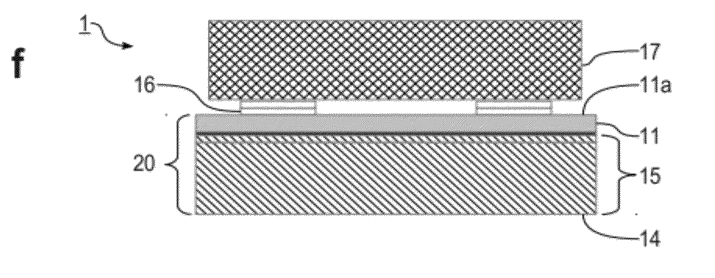
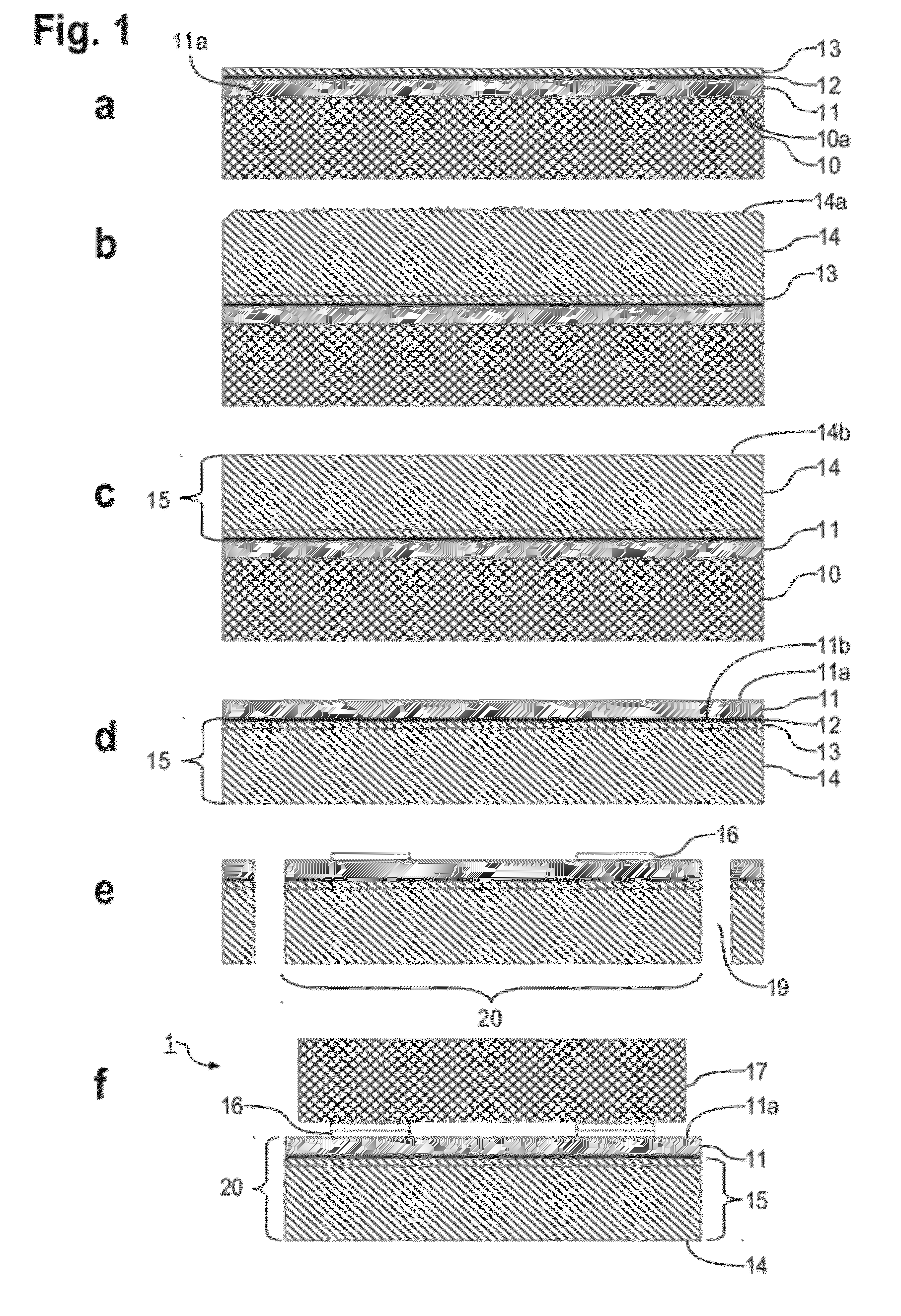
[0039]A method of fabricating a device structure 1 comprising a diamond on metal substrate or submount 20 according to the invention is illustrated in FIGS. 1a to 1f. The resulting device structure 1, shown in FIG. 1f, comprises a high power semiconductor device or chip 17 and a chip submount 20 comprising an HTC metal substrate 15 and a top layer 11 of HTC diamond, which has a smooth surface 11a of a required surface roughness, preferably 16 are defined on the diamond surface 11a for bonding the chip 17 to the diamond layer 11. In this embodiment, the metal substrate 15 is preferably copper and it comprises a thin first layer 13 of deposited copper, e.g. sputtered copper, which forms a plating base layer for a thicker second layer of electrodeposited copper 14. An adhesion layer 12 comprising a layer of sputtered Ta is provided between Cu layer 13 and the HTC diamond layer 11.

[0040]By using a fabrication sequence including a sacrificial polished silicon substrate, a layer 11 of lar...

second embodiment

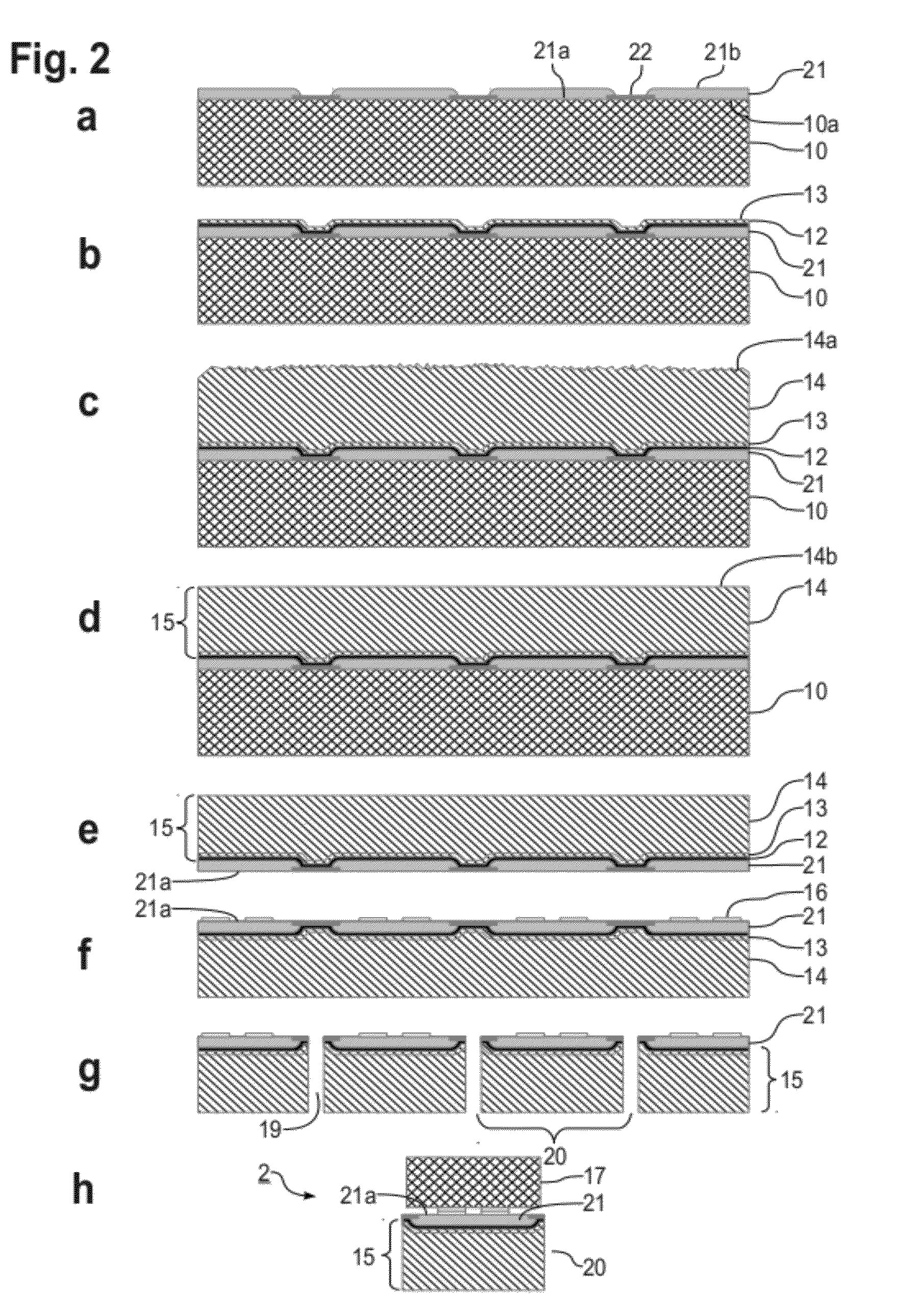
[0049]Dicing the substrate, e.g by cutting dicing streets 19 to create a plurality of thermal dissipation structures or submounts 20 (FIG. 1e), of desired sizes, can be performed either before or after the formation of the conductive leads 16. Preferred dicing methods are laser dicing or abrasive jet dicing. Alternatively, the diamond layer can be patterned by reactive ion etching (RIE) or inductively-coupled plasma RIE (ICP-RIE) through a silicon dioxide (SiO2) or other hard mask (e.g. 1-3 μm thick) as described by Moldovan et al. (Journal Vac. Sci. Technology, B, 27 (6) pp. 3125-2121, 2009), prior to dicing, to avoid dicing through the hard material. A thicker hard mask layer may be required for thicker diamond films. That is, the etch rate selectivity of the ICP-RIE process may not be sufficient if a relatively thin (˜1 um) layer of SiO2 is used as a mask with a relatively thick diamond layer (˜>5 um). Alternative dicing methods are presented in the

[0050]The resulting structure o...


PUM

PropertyMeasurementUnit
Thicknessaaaaaaaaaa
Thicknessaaaaaaaaaa
Thicknessaaaaaaaaaa

Abstract

A method of fabrication, a device structure and a submount comprising high thermal conductivity (HTC) diamond on a HTC metal substrate, for thermal dissipation, are disclosed. The surface roughness of the diamond layer is controlled by depositing diamond on a sacrificial substrate, such as a polished silicon wafer, having a specific surface roughness. Following deposition of the diamond layer, an adhesion layer, e.g. comprising a refractory metal, such as tantalum, and at least one layer of HTC metal is provided. The HTC metal substrate is preferably copper or silver, and may be provided by electroforming metal onto a thin sputtered base layer, and optionally bonding another metal layer. The electrically non-conductive diamond layer has a smooth exposed surface, preferably ≦10 nm RMS, suitable for patterning of contact metallization and/or bonding to a semiconductor device. Methods are also disclosed for patterning the diamond on metal substrate to facilitate dicing.

Description

CROSS-REFERENCE TO RELATED APPLICATION(S)[0001]This application claims priority from U.S. provisional patent application Ser. No. 61 / 466,760, entitled “Chip submounts made of diamond on metal substrates for thermal dissipation and method of fabrication” filed Mar. 23, 2011, by the present inventors, which is incorporated herein by reference, in its entirety.TECHNICAL FIELD[0002]This invention relates to thermal management of devices using heatsinks and more particularly relates to fabrication of device structures and submounts comprising diamond on metal for thermal management of semiconductor devices, such as high power semiconductor devices.BACKGROUND ART[0003]The reliability, performance, power consumption and other factors in the operation of high power semiconductor devices, such as high power Light Emitting Diodes (LEDs), high capacity Central Processing Units (CPUs), power amplifiers, and other devices, are often limited by thermal management capabilities for dissipation of h...

Claims


Application Information

Patent Timeline
IPC IPC(8): H01L23/373H01L21/50B32B33/00C25D1/00B32B7/12B32B9/04
CPCC25D1/04Y10T428/24355C25D3/38C25D3/46C25D3/58C25D3/64C25D5/10C25D5/48H01L23/142H01L23/3732B32B37/26C23C16/01C23C16/0281C23C16/042C23C16/27B32B2037/246B32B2037/268B32B2309/105B32B2311/00B32B2313/04H01L2924/0002C25D1/08Y10T428/24975Y10T428/24942H01L2924/00C09K5/14C01B32/28C25D5/611H01L2924/12042H01L2924/15747Y10T428/31678C25D1/00H01L21/4878H01L21/4882H01L24/81H01L2924/01022H01L2924/01029H01L2924/01041H01L2924/01042H01L2924/01047H01L2924/01073H01L2924/01074H01L2924/0132
Inventor MOLDOVAN, NICOLAIE A.CARLISLE, JOHN ARTHURZENG, HONGJUN
Owner ADVANCED DIAMOND TECH
Why Eureka
Try Eureka