Method and composition for selectively removing metal hardmask and other residues from semiconductor device substrates comprising low-k dielectric material and copper

a technology of semiconductor devices and substrates, applied in the direction of inorganic non-surface active detergent compositions, cleaning using liquids, instruments, etc., can solve the problems of reducing the useful life of composition baths and pots, affecting the critical profile control of vias and trenches, and affecting the performance of the composition. , to achieve the effect of reducing the rate of oxidizer decomposition, extending the useful life of composition baths and pot life, and high etch ra

Inactive Publication Date: 2015-04-16
EKC TECH
View PDF2 Cites 31 Cited by
  • Summary
  • Abstract
  • Description
  • Claims
  • Application Information

AI Technical Summary

Benefits of technology

[0027]A composition formulated according to the invention and exhibiting an inherently high etch rate for TiN, TaN, TiNxOy, TiW and W, including alloys of Ti and W, enables processing at relatively low temperature, e.g., temperatures less than 65° C. A relatively low temperature process exhibits a reduced oxidizer decomposition rate, which, in turn, extends the useful composition bath life and pot life. Additionally, compositions according to the invention which exhibit high and selective etch rates for TiN, TaN, TiNxOy, TiW and W, including alloys of Ti and W, are desirable because they can reduce device processing time and thereby increase throughput. Typically, high etch rates for TiN, TaN, TiNxOy, TiW and W, including alloys of Ti and W, have been achieved by increasing process temperatures. However, for single wafer process applications, the highest processing temperature is around 75° C., which, in turn, can limit the upper end of etch rates for TiN, and thereby limit the ability for one to completely remove TiN metal hardmask from a dual damascene structure. Compositions according to the invention can effectively deliver high etch rates for TiN, TaN, TiNxOy, TiW and W, including alloys of Ti and W, with single wafer tool applications at a temperature range of from 20° C. to 60° C., and the TiN, TaN, TiNxOy, TiW and W, including alloys of Ti and W, metal hardmask can be fully removed with single wafer application process equipment if so desired.

Problems solved by technology

As the technology nodes advance to 45 nm and smaller, the decreasing size of the semiconductor devices makes achieving critical profile control of vias and trenches more challenging.
Fabrication of advanced generation devices that require copper conductors and low-k dielectric materials (typically carbon-doped silicon oxide (SiOCH), or porous low-k materials) give rise to the problem that both materials can react with and be damaged by various classes of prior art cleaners.
Low-k dielectrics, in particular, may be damaged in the cleaning process as evidenced by etching, changes in porosity / size, and ultimately changes in dielectric properties.
Some residues may be cleaned in a very short period of time, while some residues require much longer cleaning procedures.

Method used


Image

  • Method and composition for selectively removing metal hardmask and other residues from semiconductor device substrates comprising low-k dielectric material and copper
  • Method and composition for selectively removing metal hardmask and other residues from semiconductor device substrates comprising low-k dielectric material and copper
  • Method and composition for selectively removing metal hardmask and other residues from semiconductor device substrates comprising low-k dielectric material and copper

Examples


examples

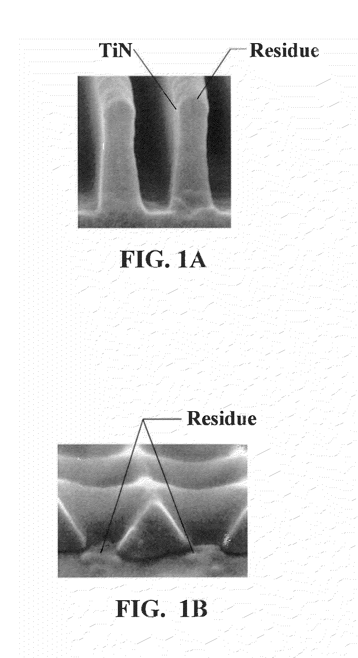
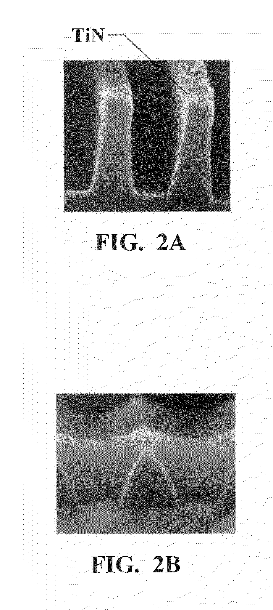
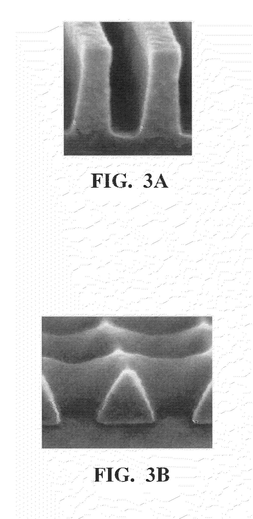
[0050]Removal compositions according to the invention are now explained in detail by reference to the inventive concepts and examples which follow, but the present invention is not limited by these examples and the results shown for each test. Compositions of the invention may be embodied in a wide variety of specific formulations, as hereinafter more fully described. In all such compositions, wherein specific components of the composition are discussed in reference to weight percentage ranges including a zero lower limit, it will be understood that such components may be present or absent in various specific embodiments of the composition, and that in instances where such components are present, they may be present at concentrations as low as 0.0001 wt %, based on the total weight of the composition in which such components are employed.

[0051]In the examples which follow, 100 g. samples of removal compositions were prepared according to the inventive concept(s) described herein. Ea...


PUM

PropertyMeasurementUnit
wt %aaaaaaaaaa
temperatureaaaaaaaaaa
sizeaaaaaaaaaa

Abstract

An aqueous removal composition having a pH in the range of from 2 to 14 and method for selectively removing an etching mask consisting essentially of TiN, TaN, TiNxOy, TiW, W, or alloy of Ti or W relative to low-k materials from a semiconductor substrate comprising said low-k materials having a TiN, TaN, TiNxOy, TiW, W, or alloy of Ti or W etching mask thereon wherein the removal composition comprises at least one oxidizing agent and a carboxylate compound.

Description

CROSS REFERENCE TO RELATED APPLICATIONS / INCORPORATION BY REFERENCE STATEMENT[0001]This application claims the benefit of U.S. provisional application Ser. No. 61 / 889,968, filed Oct. 11, 2013, the entire contents of which are hereby incorporated herein by reference.BACKGROUND OF THE INVENTION[0002]The presently disclosed and claimed inventive concept(s) relates to compositions and methods for selectively removing metal hardmask and other residues from integrated circuit (IC) device substrates, and, more particularly, to compositions and methods useful for selectively removing TiN, TaN, TiNxOy, TiW, and W metal hardmask, and metal hardmasks comprising alloys of the foregoing, as well as other residues from such substrates comprising low-k dielectric materials, TEOS, copper, cobalt and other low-k dielectric materials, using carboxylate compounds.[0003]Devices with critical dimensions on the order of 90 nanometers (nm) have involved integration of copper conductors and low-k dielectric...

Claims


Application Information

Patent Timeline
Patent Type & Authority Applications(United States)
IPC IPC(8): G03F7/42H01L21/033
CPCG03F7/423H01L21/0337H01L21/02063H01L21/31144H01L21/32134C23F1/18C23F1/26C23F1/28C23F1/34C23F1/38C23F1/40C11D3/3947C11D7/265C11D7/3245G03F7/425G03F7/426C11D11/0047C11D7/3281C11D7/3218C11D7/3209C11D7/50C11D7/04H01L21/31111B08B3/08H01L21/02057B08B3/10C11D3/2082C11D3/3942H01L21/76807H01L21/76814
Inventor CUI, HUA
Owner EKC TECH
Why Eureka
Try Eureka