Methodology for improved semiconductor process monitoring using optical emission spectroscopy

Inactive Publication Date: 2000-04-04
ADVANCED MICRO DEVICES INC
View PDF11 Cites 53 Cited by
  • Summary
  • Abstract
  • Description
  • Claims
  • Application Information

AI Technical Summary

Problems solved by technology

Turnaround time on SEM-analyzed wafers is usually long enough to allow a significant number of product wafers to pass through a contaminated chamber, which results in lower product yields or lower throughput.
But if done more often than necessary, valuable time is consumed in tool downtime and consequent tool unavailability.
PM's are frequently performed after a set number of wafers, whether needed or not, due to the difficulty and time delay of ascertaining whether etch stop conditions are present within the tool chamber.
One of the difficulties of using OES in a semiconductor process is the large number of spectral lines present

Method used


Image

  • Methodology for improved semiconductor process monitoring using optical emission spectroscopy
  • Methodology for improved semiconductor process monitoring using optical emission spectroscopy
  • Methodology for improved semiconductor process monitoring using optical emission spectroscopy

Examples


Example

)

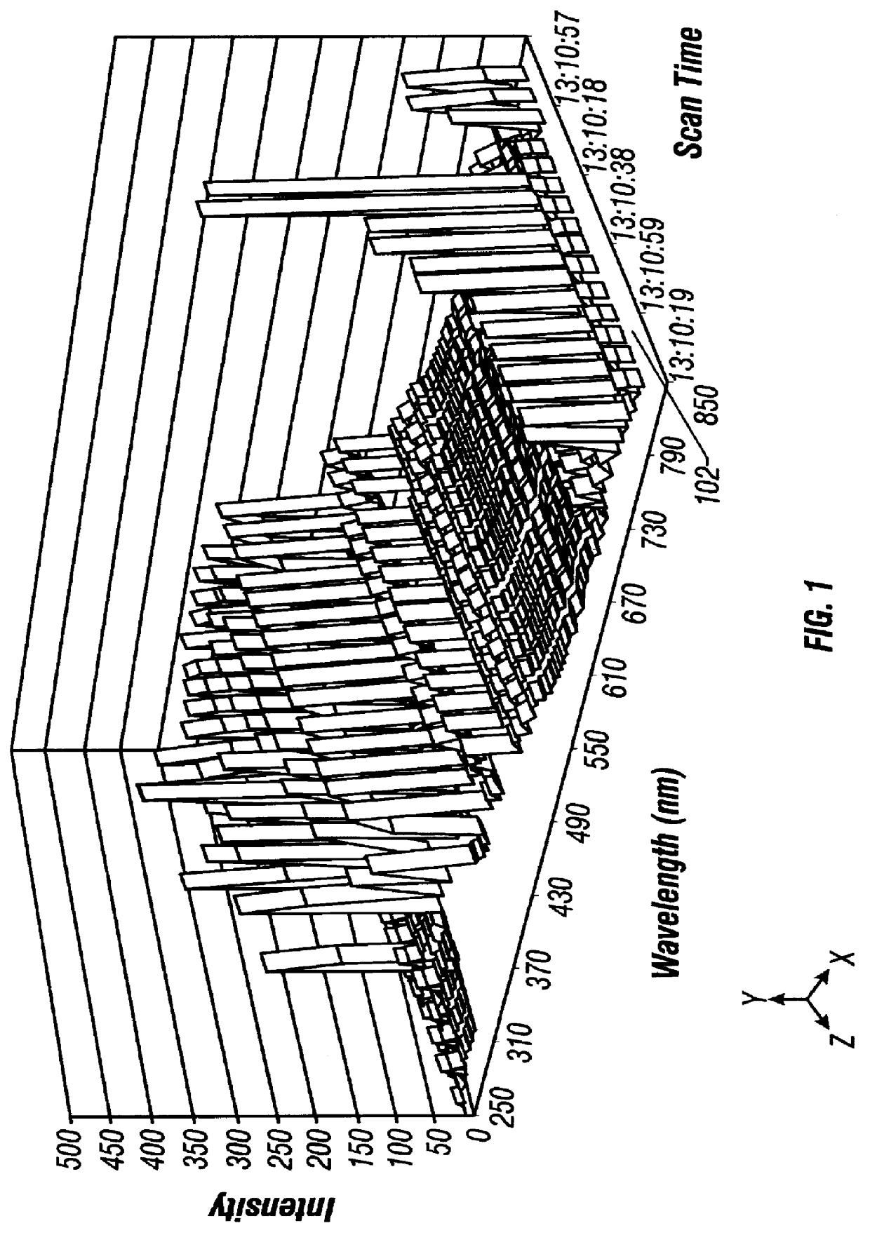
An Applied Materials 5300 HDP Etcher was used to study the correlation of OES data to the determination of etch stop conditions during a contact / via etch performed through an inter-metallic dielectric layer, such as an oxide. An SC Technology OES Monitor was attached to the viewing port of the plasma etcher and which transmits light to a photodiode array via a fiber optic cable. A diffraction grating of 150 grooves / mm was used to provide spectral intensity sampling of approximately 500 individual wavelengths within the range of 200 to 900 nm.

FIG. 1 illustrates the observed spectral intensities at various times during a particular oxide etch, as measured on a photoresist-covered dummy wafer. The observed wavelengths range from approximately 250 to 850 nanometers (as plotted along the x-axis). The intensity of the wavelengths are shown on the y-axis, and the time elapsed during the etch shown on the z-axis. Sixteen (16) scans are shown, each taken at approximately 10 second intervals...


PUM


Abstract

In a semiconductor process which utilizes a plasma within a process tool chamber, a method of using optical emission spectroscopy (OES) to monitor a particular parameter of the process is disclosed. A first wavelength present in the plasma is determined which varies highly in intensity depending on the particular parameter by observing a statistically significant sample representing variations of the particular parameter. A second wavelength of chemical significance to the process is also determined which is relatively stable in intensity over time irrespective of variations of the particular parameter, also by observing a statistically significant sample representing variations of the particular parameter. These two wavelengths may be determined from test wafers and off-line physical measurements. Then, the intensity of the first and second wavelengths present in the plasma is measured on-line during normal processing within the process tool chamber, and the ratio between the first and second wavelength's respective intensities generates a numeric value which is correlated to the particular parameter. As an example, such a method may be used to generate a reliable alarm signal indicating the presence of etch stop conditions within a plasma oxide etcher, as well as to indicate the oxide etch rate.

Description

1. Field of the InventionThis invention relates to semiconductor manufacturing, and more particularly relates to the monitoring of semiconductor process operations which use a plasma within a chamber by observation of the light produced by the plasma.2. Description of the Related ArtOptical Emission Spectroscopy (OES) is a process by which light emitted by a process, such as a plasma within a semiconductor reaction chamber, is analyzed to see which wavelengths are present in the light. Inferences about the process may then be drawn as a result of the intensity of the various spectral lines present in the light. For example, the presence of certain species within the chamber may be ascertained. OES may be used with any chamber which provides a window through which light present within the chamber may be observed. This allows use of OES even with processes having very corrosive gases present, or processes accomplished at very low or very high pressures. This non-intrusive nature is a ...

Claims


Application Information

Patent Timeline
IPC IPC(8): H01L21/66H01J37/32
CPCH01J37/32935H01L22/26H01J37/32972
Inventor MARKLE, RICHARD J.GATTO, MICHAEL J.NAUERT, CHRIS A.CHENG, YIPATTY, RICHARD B.
Owner ADVANCED MICRO DEVICES INC
Why Eureka
Try Eureka