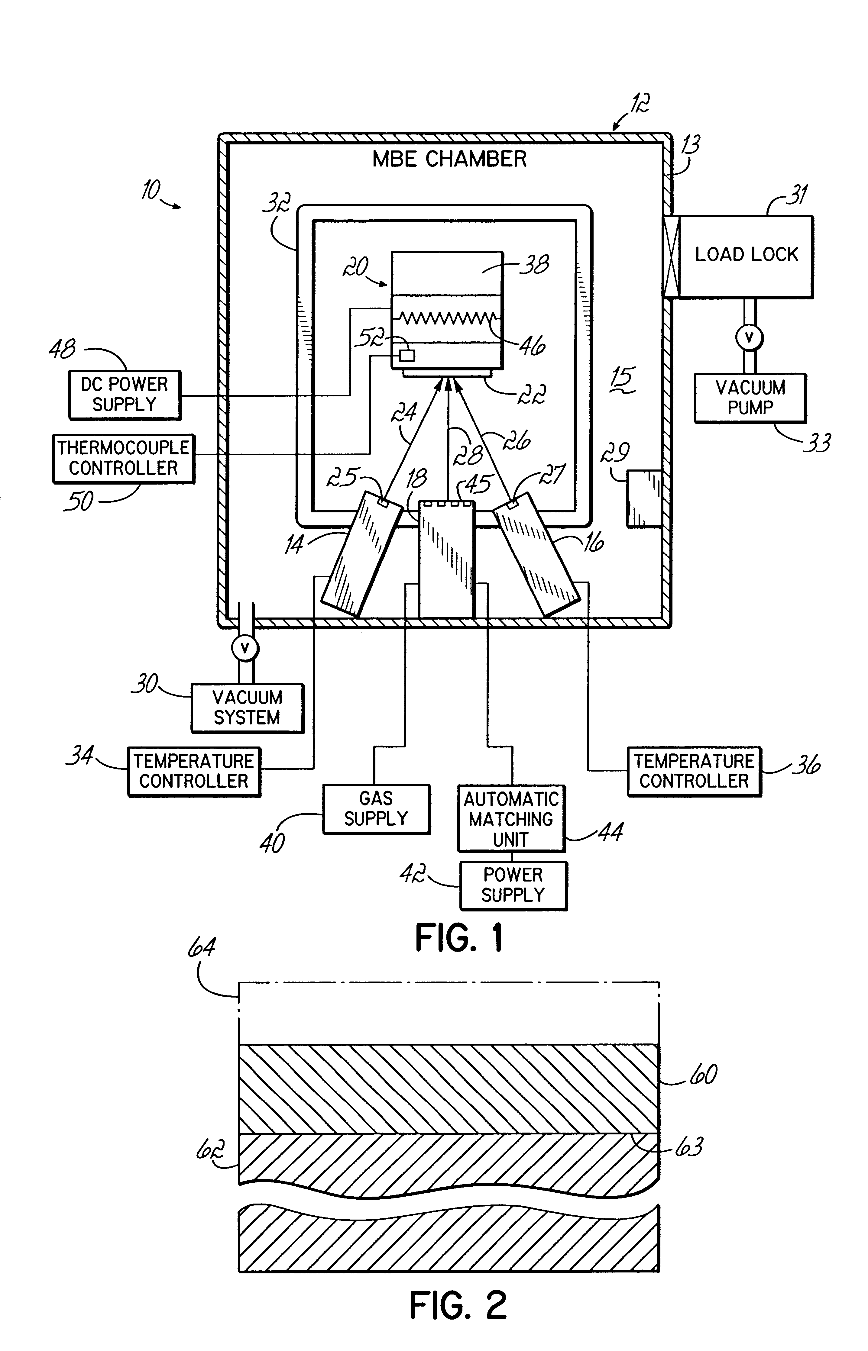
Each of the
effusion cells 14, 16 has an individual mechanical
shutter (not shown) controllably movable into and out of the respective beam path for selectively initiating and terminating the
exposure of the substrate 22 to the molecular beams 24, 26 selectively. A primary mechanical
shutter (not shown) provided
proximate the substrate 22 is selectively positionable for isolating substrate 22 by blocking molecular beams 24, 26. The configuration of the substrate holder 20 and the mechanical shutters accurately control the duration of the
exposure of substrate 22 or beam flux monitor 38 to either of the beams 24, 26 and, thus, contribute to close control of the formation of the epitaxial layer on substrate 22.
Before depositing the ZnO layer, the exposed surface of substrate 22 may be prepared with an in situ cleaning process. A typical in situ cleaning process involves heating the substrate 22 to a temperature in the range of about 500.degree. C. to 850.degree. C., perhaps with a ramped temperature profile or schedule, and contemporaneously exposing the surface to an active flux 28 of
atomic species, such as a mixture of radicals, neutrals, ions, and molecules of
hydrogen and
oxygen, generated from a mixture of
hydrogen and
oxygen process gases by RF
plasma source 18. The cleaning process promotes adhesion of the deposited layer to substrate 22, promotes crystalline alignment of the lattice structure of the layer with the substrate 22, and improves the crystalline quality of the lattice structure of the deposited ZnO layer by
etching a thin
surface layer for reducing potential defect centers.
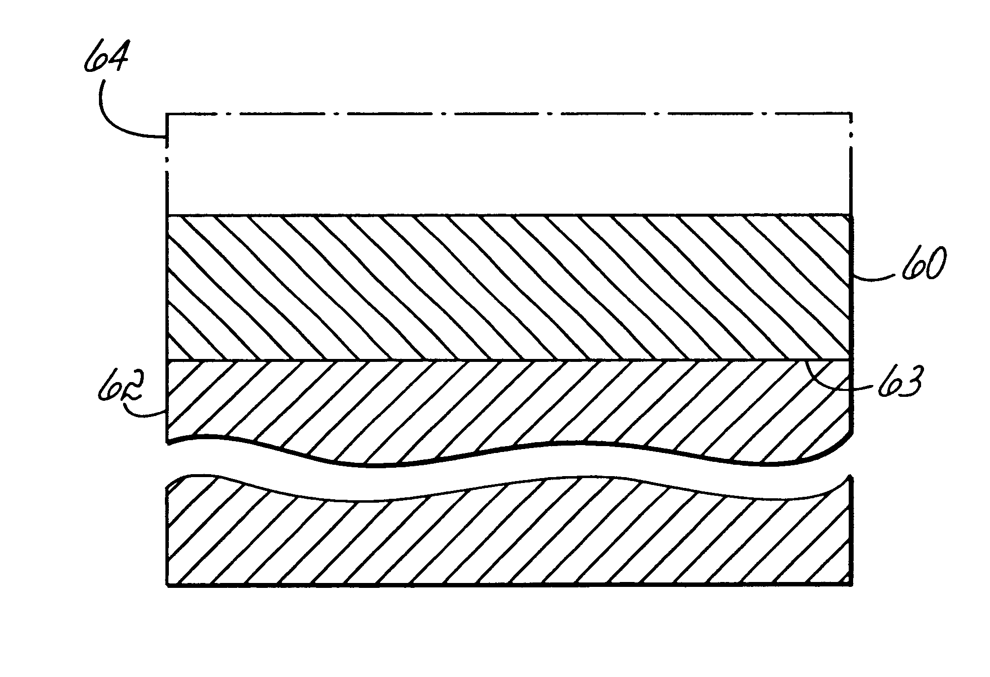
As is generally accepted, zinc oxide incorporates a significant excess concentration of uncompensated carriers (donors), which significantly lowers the resistivity of the material and results in n-type conduction. According to the principles of the present invention, the atomic concentration of the compensating
dopant creates deep-level traps in the p-type ZnO layer 60, which promote recombination of the excess donors to effectively compensate for the excess donor concentration. The p-type dopant independently provides the acceptors that create p-type conduction in the ZnO layer 60. In one aspect of the invention, the incorporation of the compensating dopant into the crystalline structure of the ZnO layer 60 reduces the atomic concentration of p-type dopant required to provide the desired carrier concentration.
In certain embodiments of the present invention, the compensating dopant is diffused into the ZnO substrate 62 before the p-type ZnO layer 60 is deposited. As a specific example, an atomic concentration of Li is drifted or diffused at an elevated temperature into the ZnO substrate 62. The Li atoms compensate for the carrier imbalance in the ZnO substrate 62 so that, following the Li-drifting procedure, the ZnO substrate 62 has a low net concentration of uncompensated carriers and an enhanced resistivity. During deposition, ZnO substrate 62 is heated to the desired
deposition temperature and Li atoms are transported by
diffusion from the ZnO substrate 62 into the ZnO layer 60. It is appreciated that the
diffusion of Li from the ZnO substrate 62 into the ZnO layer 60 may be induced by a post-deposition thermal anneal in a
vacuum furnace at a given
diffusion temperature, for example, in the range of about 525.degree. C. to about 800.degree. C., for which any p-type dopant in the ZnO layer 60 is not adversely affected.
Homoepitaxial deposition of the p-type ZnO layer 60 on ZnO substrate 62 provides ZnO layer 60 with excellent bulk and surface microstructures, uniform and optimized
doping, and optical and electrical properties that are reproducible in successively deposited layers and enhances the properties of devices made on and / or in layer 60. The morphology of the
microstructure of the ZnO layer 60 is enhanced because layer 60 is substantially lattice matched to the ZnO substrate 62 and because layer 60 and substrate 62 have substantially identical coefficients of thermal expansion. As a result, homoepitaxy on
single crystal ZnO substrate 62 significantly reduces the number of defects, such as misfit dislocations and
threading dislocations, in the ZnO layer 60. It is known that ZnO layers deposited heteroepitaxially on diverse substrates, such as
gallium arsenide,
silicon or sapphire, have large mismatches in lattice parameters with the substrate and differing coefficients of thermal expansion that contribute to the introduction of significant numbers of misfit and
threading dislocations into the deposited ZnO layers. In addition, the improvement in the crystalline quality manifested by the reduction in defect density resulting from the homoepitaxial deposition of ZnO layer 60 on ZnO substrate 62 allows the introduction of a higher concentration of uncompensated donors and an enhanced probability of obtaining uncompensated acceptors and p-type
conductivity. The ZnO layer 60 is substantially free of surface imperfections that can cause
device failure and provides for increased reliability of the finished
semiconductor device and greater efficiencies during the semiconductor manufacturing process.
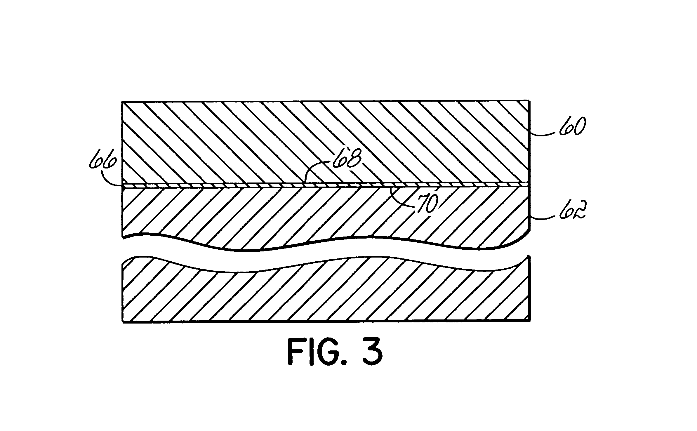
In certain embodiments, the buffer layer 66 may operate as a
diffusion barrier that reduces or limits the diffusion of the compensating dopant from the ZnO substrate 62 into the ZnO layer 60. In other embodiments, the buffer layer 66 may operate as an active layer in a
semiconductor structure formed on ZnO substrate 62. In still other embodiments, the buffer layer 66 may be provided as an intermediate layer that effectively improves the crystalline quality of ZnO substrate 62 before depositing ZnO layer 60.

