
Small-scale optoelectronic package

a small-scale optoelectronic and package technology, applied in the direction of instruments, optical elements, semiconductor/solid-state device details, etc., can solve the problems of difficult to efficiently configure the light path between the optical fiber and the optoelectronic device, space constraints, and the like, to achieve the effect of being easily manufacturable and not sacrificing speed and power performan

Inactive Publication Date: 2005-06-28
PSEMI CORP
View PDF30 Cites 223 Cited by
  • Summary
  • Abstract
  • Description
  • Claims
  • Application Information

AI Technical Summary

Benefits of technology

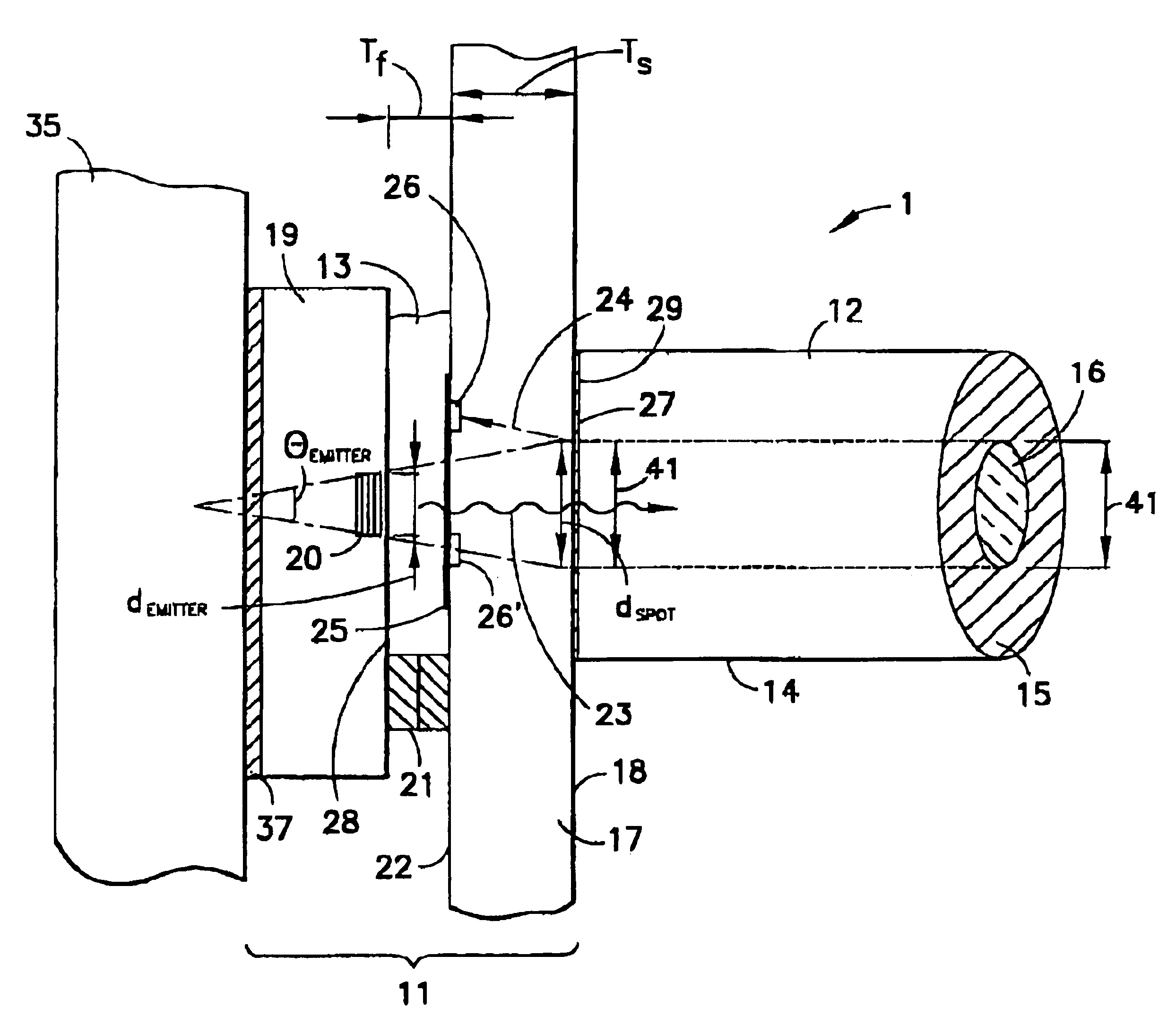
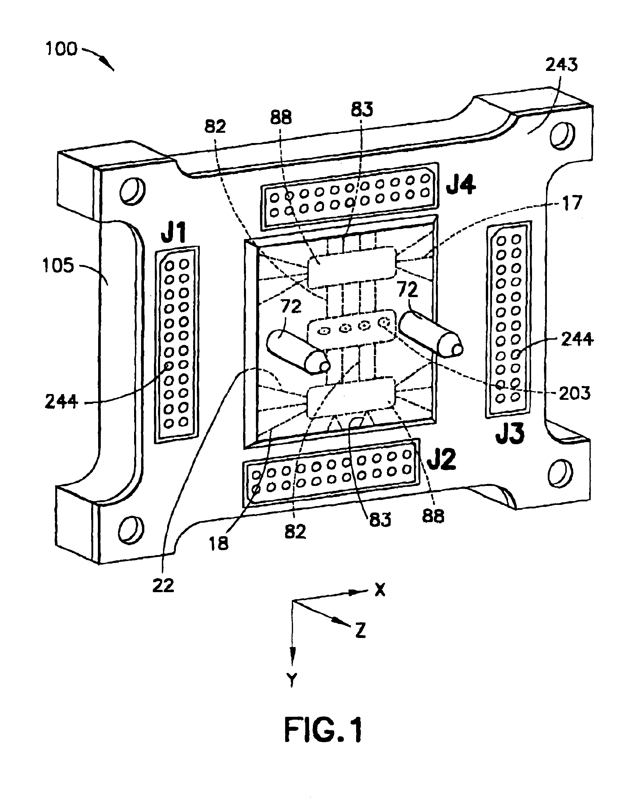
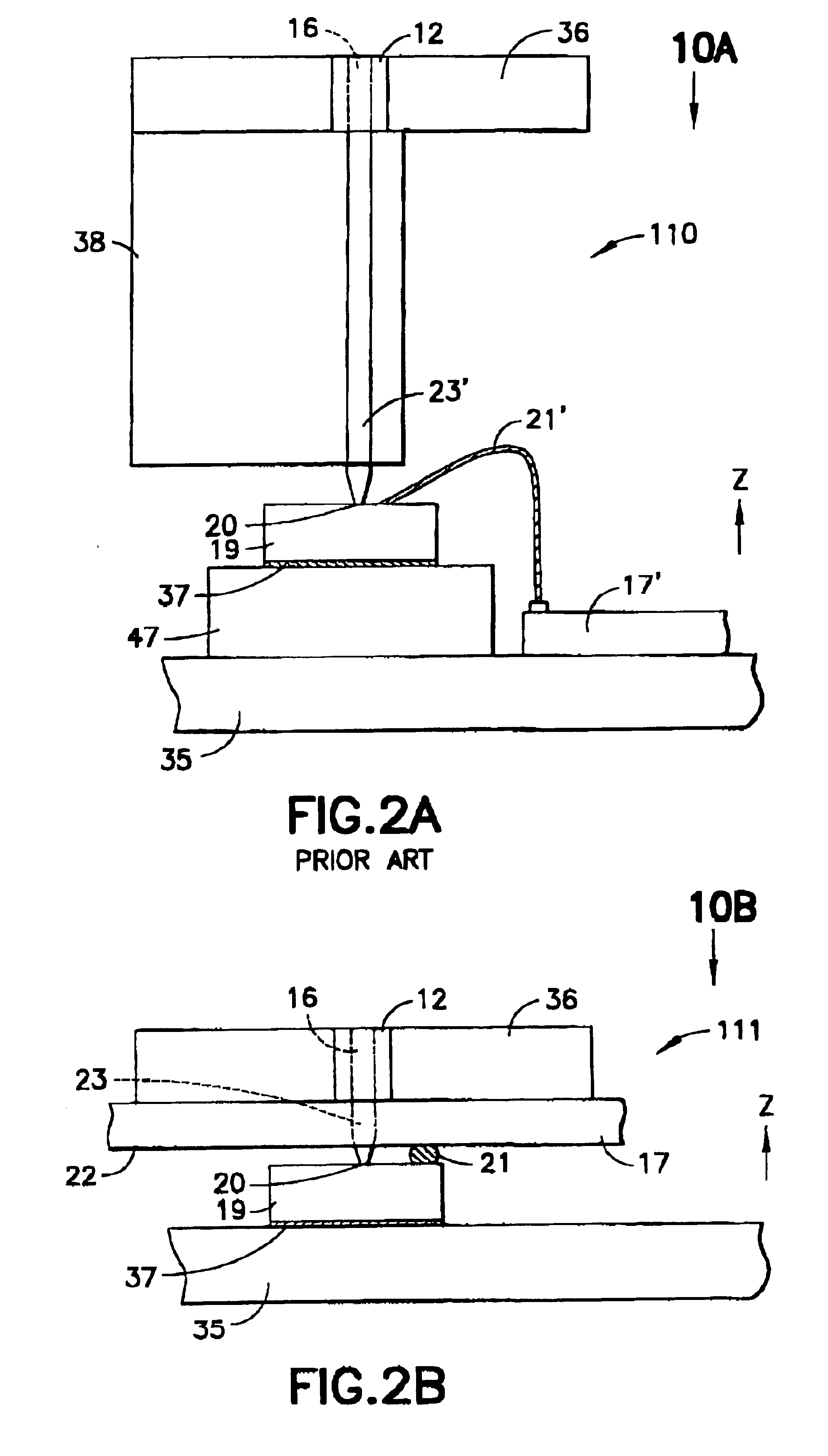
The present invention provides a method for packaging and aligning optical fibers and optoelectronic devices, allowing for high-speed and high-power performance. The invention overcomes the limitations of previous methods that sacrificed speed and power performance. The invention includes a transparent insulating substrate with a thin layer of silicon on its top surface, which has a conductive circuit integrated with the optoelectronic device. The optical fiber is held in a precise positional relationship to the substrate, and the substrate is positioned between the optical fiber and the optoelectronic device. The invention also includes a method for fabricating the optical / optoelectronic coupling structure, which includes an optical fiber, an optoelectronic device, and a transparent insulating substrate. The optoelectronic device can be a laser, photodetector, or modulator, with VCSELs being of special interest. The invention provides a simple and passive alignment of optical fibers to optoelectronic devices, resulting in high-rate optical transmission with low optical loss and low electrical parasitics.

Problems solved by technology

Applications that require manipulation of many optical signals are becoming more complex and more commonplace.
Therefore, space constraints figure strongly in the design of packages that integrate electronic functions with optoelectronic devices.
The requirement to make electrical contact to the optoelectronic device on the same side as the region to which light must have access makes it difficult to efficiently configure the light path between the optical fiber and the optoelectronic device, taking into account the need for high speed electronic circuitry for driver or amplifier, control, and I / O functions.
Because of the space required for the wire bond, the optical fiber end surfaces cannot be brought flush with or sufficiently close to the optoelectronic devices to make a low-loss optical connection.
Wire bonds are often the most physically fragile part of an electronic package.
Furthermore, wire bonds introduce parasitic resistance, capacitance and inductance hence increased power dissipation.
Even for relatively low numbers of integrated optoelectronic devices, wire bonding imposed severe penalties on bandwidth and power dissipation.
More closely integrating the electrical circuits with the optoelectronic devices has the potential to increase speed and reduce losses, but close integration must not lead to excessive heat transfer from the electrical circuits to relatively heat-sensitive OE devices and consequent performance degradation.
To date, various methods to integrate electronic and optoelectronic functions have been tried, with less than ideal results.
Heteroepitaxial growth of GaAs on silicon, and silicon on GaAs have been explored, but after decades of research, fundamental problems such as the mismatch in the crystal lattice constants, cross-contamination, incompatibilities of device processing, and the difference in the coefficients of thermal expansion of the two materials have prevented this goal from being satisfactorily achieved on a commercial scale, particularly when high performance lasers, photodetectors or drive electronics are required.
Epoxy casting, by which completely fabricated chips are mounted in a common epoxy cast and final metal deposited (multi-chip modules) has numerous problems, including high cost and poor parasitics, size, reliability and yield.
Selectively etching optical access areas to provide light paths to an array of OE devices is a demanding and unattractive manufacturing step.
Furthermore, infrared detectors are generally low speed systems, often operating at Kilohertz speeds.
These high speeds cause the silicon substrate parasitics to become significant in areas of power consumption, crosstalk, distortion, maximum frequency and noise.
These electrical limitations of silicon as a substrate material are true for all wavelengths of light being used.
Therefore, even if the silicon is transparent at a given wavelength, it is not an ideal substrate for high speed (multi-Gigahertz) optical communication systems.
However, these highly automated and precise methods have not heretofore been applied to assembling structures that incorporate integrated circuit chips and optoelectronic devices, packaged in a form that allows for the optoelectronic devices to be readily aligned to optical fibers for forming optical interconnections.
During manufacturing, complex manipulations in three dimensions are required, and the low cost automated assembly and testing techniques are not applicable to all the steps involved in assembling and packaging all the components of an optical data link.
Alignment of the optoelectronic device and optical fiber may be a manual or relatively expensive hybrid manufacturing step.
Furthermore, current methods of packaging optoelectronic devices with the associated integrated circuits used for control of the optoelectronic devices do not allow for handling, test and burn-in at the chip scale package level.
The optoelectronic devices cannot be “burned in” (stressed at conditions that are designed to simulate extreme conditions the product may encounter and provoke any failures that could occur) and tested under operating conditions until a late stage of manufacturing.
Burn-in and test at a late stage, when the components—optoelectronic device die, integrated circuit die, alignment means—have been mounted and assembled into a module, results in yield loss of fully packaged components, leading to overall higher costs.

Method used


Image

  • Small-scale optoelectronic package
  • Small-scale optoelectronic package
  • Small-scale optoelectronic package

Examples


Embodiment Construction

Definitions

[0113]As used herein, the following terms are defined as follows:

[0114]The “transparent insulating substrates” useful in the practice of the invention include those transparent, electrically insulating substrates on which may be formed silicon layers suitable for electronic circuitry as well as transparent, electrically insulating substrates such as glass that are well-suited to bonding to integrated circuit chips.

[0115]Integration of silicon and optoelectronic devices on a common insulating transparent substrate requires that an effective method for forming silicon CMOS devices on the transparent, insulating substrate be used. Examples of and methods for making such silicon-on-sapphire devices are described in U.S. Pat. No. 5,416,043 (“Minimum charge FET fabricated on an ultrathin silicon on sapphire wafer”); U.S. Pat. No. 5,492,857 (“High-frequency wireless communication system on a single ultrathin silicon on sapphire chip”); U.S. Pat. No. 5,572,040 (“High-frequency wi...


PUM


Abstract

An integrated circuit / optoelectronic packaging system (100) which comprises OE and IC components packaged to provide electrical input / output, thermal management, an optical window, and precise passive or mechanical alignment to external optical receivers or transmitters. A transparent insulating substrate having electrical circuitry in a thin silicon layer formed on its top side is positioned between the optical fiber and the optoelectronic device such that an optical path is described between the optoelectronic device and the optical fiber core through the transparent insulating substrate. The optoelectronic devices are mounted on the transparent insulating substrate in a precise positional relationship to guide holes in the substrate. The optical fibers are fixed in an optical fiber connector and are held in a precise positional relationship to guide holes in the connector. Alignment is accomplished with complementary guide pins that pass through guide holes in the fiber optic connector and in the transparent substrate.

Description

CROSS-REFERENCE TO RELATED APPLICATIONS[0001]This application claims the priority of U.S. Provisional Patent Applications Ser. Nos. 60 / 291,348, filed May 15, 2001; 60 / 303,695, filed Jul. 6, 2001; 60 / 304,387, filed Jul. 9, 2001; 60 / 335,021, filed Oct. 31, 2001; and 60 / 365,599, filed Mar. 18, 2002.FIELD OF THE INVENTION[0002]The present invention relates to a method and apparatus for coupling light between optical fibers and optoelectronic devices and aligning the optical fibers and optoelectronic devices, for coupling light therebetween, having applicability to the manufacture of a small scale package for an optoelectronic device or arrays of such devices that provides precise alignment and efficient optical coupling.BACKGROUND OF THE INVENTION[0003]The disclosure of U.S. Provisional Patent Applications Ser. No. 60 / 291,348, filed May 15, 2001; 60 / 303,695, filed Jul. 6, 2001; 60 / 304,387, filed Jul. 9, 2001; 60 / 335,021, filed Oct. 31, 2001; and 60 / 365,599, filed Mar. 18, 2002, are here...

Claims


Application Information

Patent Timeline
Patent Type & Authority Patents(United States)
IPC IPC(8): G02B6/42
CPCG02B6/4201G02B6/4246G02B6/4277H01L2224/48091H01L2924/13091G02B6/4249G02B6/4292H01L2224/16225H01L2224/32225H01L2224/73204H01L2224/73265H01L2924/30107H01L2924/00014H01L2924/00G02B6/4259G02B6/426G02B6/4266G02B6/4269G02B6/4281G02B6/4286
Inventor POMMER, RICHARDKUZNIA, CHARLES B.LE, TRI Q.HAGEN, RICHARD T.REEDY, RONALD E.CABLE, JAMES S.ALBARES, DONALD J.MISCIONE, MARK
Owner PSEMI CORP
Learn More