
Low temperature nitridation of amorphous high-K metal-oxide in inter-gates insulator stack

Active Publication Date: 2005-08-23
PROMOS TECH INC
View PDF10 Cites 46 Cited by
  • Summary
  • Abstract
  • Description
  • Claims
  • Application Information

AI Technical Summary

Benefits of technology

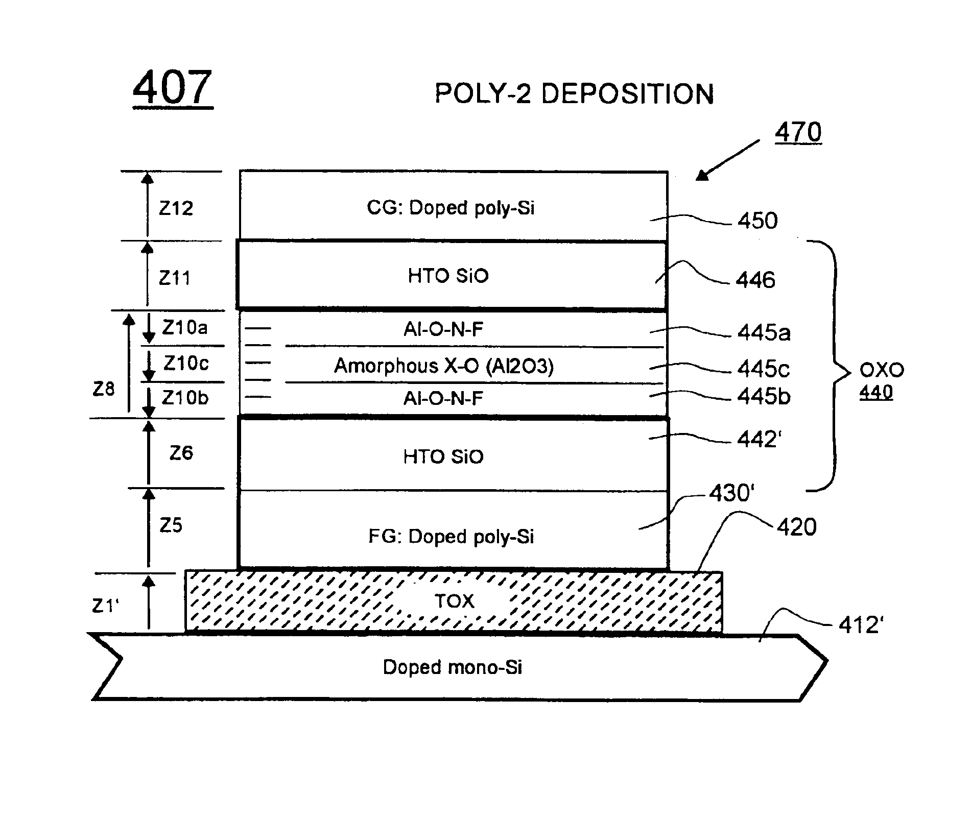
[0022]More specifically, in accordance with one aspect of the present disclosure, nitrogen atoms are incorporated into amorphous metal oxide compositions (X(a)—O) such as those compositions which contain: amorphous aluminum oxide (AlO(a)), amorphous hafnium oxide (HfO(a)), amorphous titanium oxide (TiO(a)), and / or amorphous tantalum oxide (TaO(a)) while the X(a)—O composition(s) substantially remain at relatively low temperature (e.g., less than about 330° C.), this being done so as to increase the break down voltage and / or reduce the leakage current of one or more of these amorphous constituents. The temperature(s) of the nitridation process is( / are) maintained below the recrystallization temperature(s) of the constituent amorphous metal oxides so that the high-K metal oxide(s) will substantially retain its ( / their) amorphous structure(s) during nitridation and so that they will not develop large numbers of crystal grain boundaries or otherwise undergo undesirable phase changes. Large crystal grain boundaries are undesirable because they can serve as areas of amplified electric field intensity and / or as regions where conductive impurities aggregate and they can thereby promote premature voltage breakdown or excessive current leakage. Other phase changes to the amorphous structures of the high-K metal oxides may also be undesirable because designers of mass production devices wish to obtain consistent dielectric constant values from one device to the next. By keeping temperature below a critical one or more recrystallization temperatures during the nitridation process, substantial disruption of the amorphous structures of a corresponding one or more of the high-K metal oxides may be avoided while the benefit of nitridation is obtained.
[0024]In accordance with a second aspect of the present disclosure, a downstream-microwave plasma reactor is used for introducing the nitrogen atoms at relatively low temperature (e.g., less than 330° C., this being low relative to furnace nitridation) into top and bottom surface regions of one or more layers of the amorphous metal oxide compositions while leaving an interim region, between the upper and lower regions, less disturbed. Different plasma reactors have different distribution profiles for introducing ions into thin layers of dielectric material. It has been found, for example, that the downstream-microwave processing mode of the GaSonics PEP Iridia DL™ system (GaSonics is now part of Novellus of California) tends to distribute nitrogen atoms across a 100 Å thick, dielectric layer with a distribution profile that has plural concentration peaks. More specifically, for distribution of nitrogen in silicon dioxide it was observed that a relatively low concentration of injected nitrogen occurs around the 10 Å-40 Å depth range and relatively much higher concentrations of injected nitrogen occur around the 0 Å-9 Å range and the 45 Å-60 Å range. Other types of nitridating plasma reactors have been found to have more uniform distribution for injected nitrogen across the roughly, 0 Å-100 Å depth range of silicon dioxide. For reasons that may not yet be fully understood, a multi-concentration peak injection of nitrogen atoms into a 60 Å thick, amorphous aluminum oxide layer appears to significantly improve resistance to dual-polarity breakdown. (Dual polarity refers to the challenging of the dielectric material's breakdown strength for both positive and negative voltage application across the dielectric layer.) It is possible that the increased nitrogen concentration at the top and bottom surface regions of the amorphous AlO layer seals oxygen atoms in the middle of the so-nitridated metal oxide layer an thereby preserves high-K performance. Alternatively or additionally, it is possible that the multi-peak nitrogen concentration profile between the top and bottom surface regions of the so-nitridated metal oxide layer behaves as a strong barrier to electron tunneling and thereby functions to reduce electron tunneling effects and as a consequence, improve the anti-leakage characteristics of the so-nitridated metal oxide layer. Different amounts of tunnel leakage may occur when an asymmetrically nitridated dielectric layer is subjected to stressing E-fields in both the positive and negative voltage directions. Irrespective of the correctness of such conjectured mechanisms, improved performance was observed when a below-described, dual frequency, downstream-microwave plasma reactor was used for incorporating nitrogen atoms into a high-K metal oxide layer.
[0025]In accordance with a third aspect of the present disclosure, a dual frequency, downstream-microwave plasma reactor is further used for introducing fluorine atoms at relatively low temperature (e.g., less than 330° C., this being low relative to furnace driven introductions) into the amorphous, metal oxide layer (e.g., AlO(a) layer) prior to introducing the nitrogen atoms. It is believed that the introduced fluorine atoms break or weaken metal-to-oxygen bonds (X—O bonds) in the amorphous, metal oxide layer (XO(a)) and thereby encourage the formation of a greater number of metal-to-nitrogen bonds (X—N bonds) when the nitrogen atoms are subsequently introduced, also at relatively low temperature. The relatively low temperatures of the combined fluorination and nitridation plasma treatments are believed to help preserve the amorphous character of the metal oxide layer. This in turn, it is believed, works to inhibit the formation of large, field-concentrating grain boundaries in the inner regions of the amorphous metal-oxide structure and thereby also helps to inhibit premature electric insulation breakdown.

Problems solved by technology

Because of the way the layers stack, an undesirable charge leakage path may form between the floating gate electrode (FG) and the control gate electrode (CG), passing through the IGI layer (inter-gates insulator layer).
Persons skilled in the art further appreciate that real-world insulators are generally not perfect.
Small amounts of charge can undesirably leak through them due to unintended tunneling and / or other mechanisms.
The insulator materials which are intended to keep charge bottled up in the FG can undergo unwanted high voltage breakdown if field intensity becomes too large in certain regions.
Charge stored in the floating gate (FG) may then undesirably increase or decrease when this happens.
Contaminating chemicals can pass into pinhole or other defects in the insulators and undesirably change their characteristics.
This too can create problems.
Guarding against all these possibilities is difficult, particularly as device dimensions shrink and performance demands increase.
However, the inter-gates insulator layer (IGI) that is sandwiched between the FG and the CG still suffers from problems.
The inter-gates insulator layer (IGI) is particularly prone to problems with charge leakage and breakdown as already mentioned.
Despite improvements in vapor deposition and other techniques, the ONO approach still suffers from the presence of small leakage currents between the FG and the CG.
Precise control of ONO thickness and control of material quality within the ONO stack also remains a problem.
Possible candidates for the EOT reducing materials includes oxides of certain metals such as oxides of Al, Hf, Ti, Ta, Zr, La and Y. Unfortunately, despite their relatively high-K values, many of these metal oxide compositions posses other electrical and / or mechanical characteristics which are problematic.
Among the problems are low break down voltage and high leakage current.
Large crystal grain boundaries are undesirable because they can serve as areas of amplified electric field intensity and / or as regions where conductive impurities aggregate and they can thereby promote premature voltage breakdown or excessive current leakage.
Other phase changes to the amorphous structures of the high-K metal oxides may also be undesirable because designers of mass production devices wish to obtain consistent dielectric constant values from one device to the next.

Method used


Image

  • Low temperature nitridation of amorphous high-K metal-oxide in inter-gates insulator stack
  • Low temperature nitridation of amorphous high-K metal-oxide in inter-gates insulator stack
  • Low temperature nitridation of amorphous high-K metal-oxide in inter-gates insulator stack

Examples


Embodiment Construction

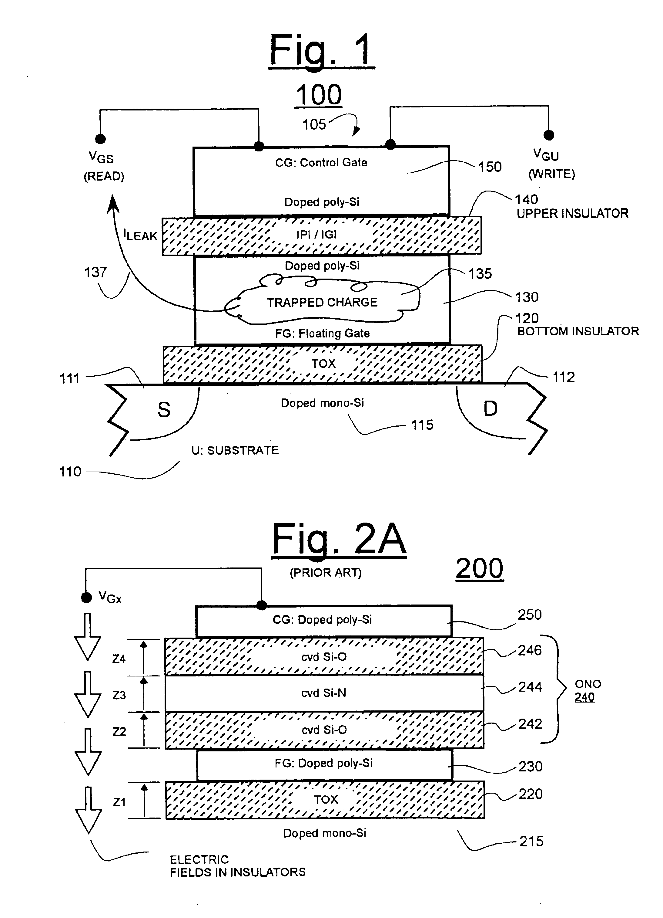
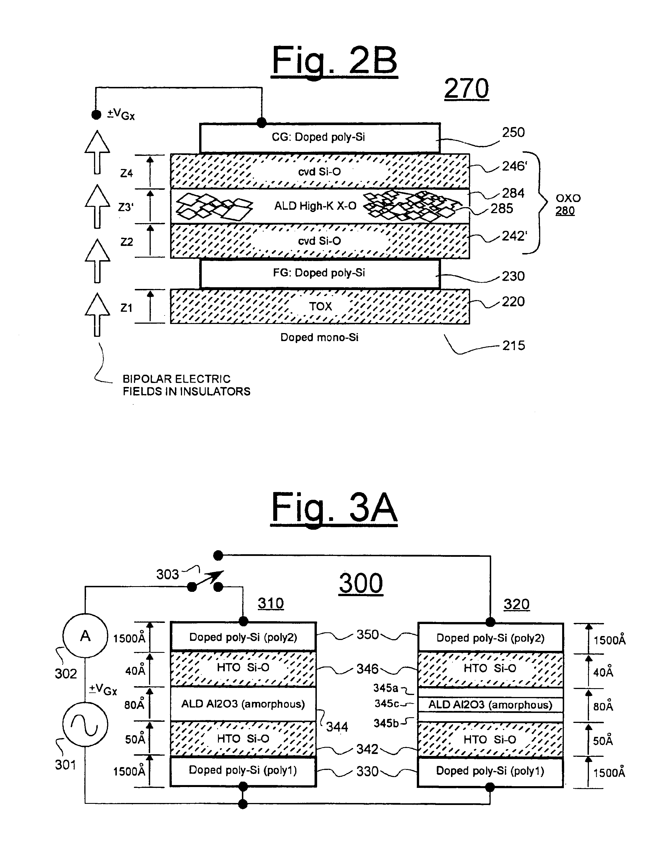
[0045]FIG. 1 is a conceptual schematic diagram showing in cross section, an environment 100 in which it may be useful to form a good, but thin, electrical insulator 140 between two conductive layers, such as two conductively-doped semiconductor layers, 130 and 150. More specifically, the not-to-scale diagram of FIG. 1 shows the structure of a stacked-gate memory cell. The cell 105 is integrally formed as part of a monolithically integrated circuit having a common substrate 110. In one embodiment, the substrate 110 includes doped monocrystalline silicon. Spaced apart source (S) 111 and drain (D) 112 regions may be formed by the implant of suitable doping elements at opposed ends of an oppositely doped, channel portion 115 of the monocrystalline silicon substrate 110. A relatively thin oxide layer (so-called tunnel oxide, or TOX) may be provided on the surface of the channel portion 115. Typically, the TOX is thermally grown from the underlying, monocrystalline silicon 115. (The TOX m...


PUM


Abstract

An OXO-type inter-poly insulator (where X is a high-K metal oxide and O is an insulative oxide) is defined by forming an amorphous metal oxide layer on a silicon-based insulator (e.g., a silicon oxide layer) and then nitridating at least upper and lower sub-layers of the amorphous metal oxide with a low temperature plasma treatment that maintains temperature below the recrystallization temperature of the amorphous material. Such a plasma treatment has been found to improve breakdown voltage characteristics of the insulator. In one embodiment, the metal oxide includes aluminum oxide and it is fluorinated with low temperature plasma prior to nitridation.

Description

1. FIELD OF DISCLOSURE[0001]The present disclosure of invention relates generally to semiconductor devices and to the manufacture of the same.[0002]The disclosure relates more specifically to mass production of insulated gate field effect transistors (IGFET's, MOSFET's) which have plural gate electrodes separated from one another by electrically insulative materials. Yet more specifically, it relates to ONO-like structures which can be used to separate stacked conductive gates in electrically re-programmable and nonvolatile memory devices where a metal oxide is substituted for the middle nitride of the ONO stack.2a. CROSS REFERENCE TO CO-OWNED APPLICATIONS[0003]The following copending U.S. patent applications are owned by the owner of the present application, and their disclosures are incorporated herein by reference.[0004](A) Ser. No. 10 / 071,689 filed Feb. 8, 2003 by Zhong Dong et al and which is originally entitled, “Floating Gate Nitridation”; and[0005](B) Ser. No. 10 / 243,379, fi...

Claims


Application Information

Patent Timeline
IPC IPC(8): H01L21/02H01L21/3205H01L21/28H01L21/314H01L29/51
CPCH01L21/28273H01L29/511H01L21/3143H01L29/40114H01L21/02164H01L21/02183H01L21/02178H01L21/02181H01L21/022H01L21/0228H01L21/02186H01L21/0234H01L21/02332
Inventor LEE, TAI-PENGHASELDEN, BARBARA
Owner PROMOS TECH INC
Learn More