Method for filling of a recessed structure of a semiconductor device

a semiconductor device and recessed structure technology, applied in the field of thin film processing, to achieve the effect of enhancing the overall process throughput, reducing cross contamination of elements, and efficient process sequence integration and execution

Inactive Publication Date: 2008-04-29
GADGIL PRASAD N
View PDF11 Cites 27 Cited by
  • Summary
  • Abstract
  • Description
  • Claims
  • Application Information

AI Technical Summary

Benefits of technology

[0038]In order to achieve high quality, low-cost and high-yield multilevel metallization scheme, all vapor phase processes capable of: deposition of high quality, pin-hole free and conformal copper diffusion barrier and an excellent, defect-free copper gap-filling in addition to a high-speed, high-precision excess copper and also copper diffusion barrier removal are highly essential. To achieve this, it is highly desirable to employ a flexible atomic layer chemical vapor processing reactor that can modulate the process mode from discrete flow (sequential pulsing) atomic layer to continuous flow high-rate chemical vapor phase processes in-situ in order to accelerate or tailor the processing speed, if required, to process larger dimension structures. Moreover, such a flexible atomic layer vapor processing reactor has capabilities to incorporate plasma to help process thin films at lower temperatures and also to selectively attract charged reactive species towards the substrate surface and thereby modulate the contours of the film being deposited within the etched gap structures or a recess.
[0043]Subsequent to complete removal of copper layer on the flat surface, the substrate wafer is transferred to the first substrate wafer processing reactor and the reactor is completely purged and evacuated. Next, a suitable vapor-phase isotropic barrier etching chemistry aided by a plasma is employed in discrete flow mode to remove the remaining exposed barrier on the top substrate surface. The reaction products of the chemical reaction of diffusion barrier removal are volatile compounds of the constituents of the diffusion barrier layer, which are removed under the combined action of temperature and / or vacuum from the vicinity of the substrate. Since the isotropic diffusion barrier removal process removes the same amount of diffusion barrier thickness as it was deposited in the first step of the barrier deposition process, it also helps run the first substrate wafer processing reactor in a quasi-clean state.
[0046]The overall process sequence employs dedicated wafer processing reactors to perform only one type of process chemistry, e.g. either copper processing, diffusion barrier processing and surface modification to maintain the purity of the internal environment within each reactor and to minimize any cross contamination of elements from one layer in to the other. Also, such approach can become effective by multiple reactors being clustered around a single automated substrate handler for efficient process sequence integration and execution. Moreover, one or more reactors in the cluster can be a batch processor to balance and enhance the overall process throughput. Finally, wherein a particular process time, e.g. copper deposition and removal, within the overall process sequence is substantially longer than the other processes, multiple and identical reactors for that particular process chemistry are employed in a cluster to avoid a bottleneck or backlog to balance wafer sequencing and achieve the maximum throughput.

Problems solved by technology

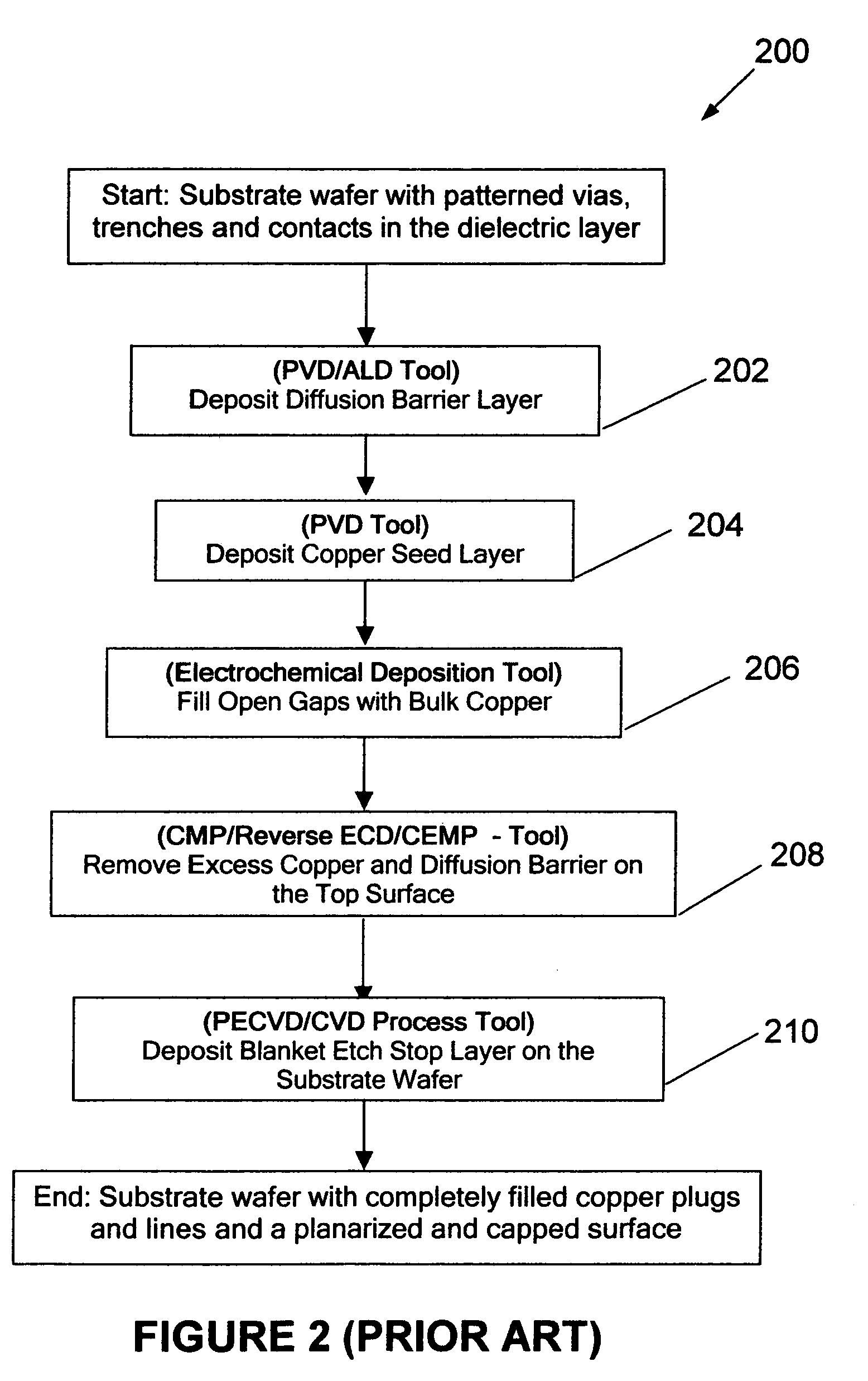
However, copper tends to diffuse in to the adjacent layers of a dielectric material during operation of the circuit under the influence of electrical field and high temperatures generated due to large operational current densities.
This can lead to short-circuiting two adjoining copper conductors and destruction of an active device.
Such a possibility can very well limit the envelope and scope of a plasma enhanced copper deposition process.
The copper precursor [Cu(thd)2] employed in this process, however, is a low volatility solid with a significantly large molecular size which may hinder surface coverage of the substrate in an ALD process.
Both copper deposition processes described above employ aqueous solutions of these chemical reagents, which makes copper susceptible to oxidation.
The aqueous process is also susceptible to difficulties encountered to transport viscous liquids into narrow sub-micron device features, which would tend to narrow further increase further with advancing device generations.
Moreover, this method of copper gap-fill does result into finite amount of copper deposition on the flat surface of the substrate which necessitates application of Chemical Mechanical Polishing (CMP) process to remove this and underlying copper diffusion barrier layer.
Apart from low volatility and potentially high cost and complexity of the copper chemical precursor molecule, the copper ALD process described above operates at higher temperature for the tolerance of delicate low-k dielectric materials.
Moreover, its reaction with atomic hydrogen can potentially reduce the ALD reaction temperature significantly.
In addition to this, atomic hydrogen tends to rapidly recombine on metal surfaces leading to its depletion in deep and narrow trenches.
Thus in absence of an efficient mechanism to transport atomic hydrogen effectively and in sufficient quantities within etched features over the entire substrate surface, it would be difficult to realize an effective copper ALD process from CuCl and atomic hydrogen.
The copper chemical precursors employed in the copper deposition processes described above are low volatility and large organometallic molecules that are generally expensive.
Moreover, their vapor phase dissociation, by application either of heat or plasma, is seldom clean and it tends to incorporate undesirable impurities such as carbon, fluorine and others that adversely affect the purity, resistivity and also adhesion of the resultant copper layer to the underlying diffusion barrier.
However the approach as outlined above has a number of serious pitfalls:(a) Inadequate step coverage by sputtering of barrier in small vias and trenches: As the critical device dimensions reduce with each advancing device generation, the vias and trenches are becoming increasingly smaller from 0.13 to 0.10 micron and even below while aspect ratio is steadily increasing.
Sputtering (PVD) being a line of sight process leads to inadequate deposition of thin film material on the side-walls of the dielectrics.
As a result, conformality of barrier deposition by this method is becoming increasingly inadequate.
This has led to significant and adverse impact on the quality of copper seed layer and subsequent copper gap fill process extending into the overall device quality.(b) Poor conformality and discontinuity of copper seed layer by sputtering: Thin copper seed layer as sputtered on the underlying diffusion barrier also shows inadequate degree of conformal deposition and at times spatial discontinuity and non-uniformities over the contours and surfaces of the structures.
However, any discontinuity in this layer has serious consequences for the next step of electrochemical copper deposition which requires a physically continuous copper layer.
Thus reliability and quality of the device in terms of important functional parameters such as electromigration resistant can be seriously compromised if this step is not performed satisfactorily.(c) Corrosion due to wet electrochemistry: This is a very serious issue that is under active investigation.
The CMP or the other processes employed to remove copper such as dissolution of copper in acidic solutions, reverse anodic electro-dissolution of copper are fraught with corrosion of copper.
Copper is highly susceptible to oxidation when exposed to moist air at room temperature.
Also, copper wiring in microcircuits during operation, as it conducts electricity, may heat up significantly.
This may result in to undesirable scenarios: generation of high pressure localized steam that may lead to violent rupture of the interconnect structure or it may set up localized galvanic cells to initiate copper corrosion.
Moreover, in-situ corrosion due photoelectrons has been an added issue.
All these factors have a significant and adverse impact on the yield, reliability and overall stability of a copper metallization interconnect scheme being practiced currently.(d) Dishing and erosion in CMP: During CMP the wafer surface is polished by rotating and pressing it against a flexible pad on to which an aqueous slurry containing a chemically active agent (chlorides of iron etc.) and an abrasive powder (such as ceria—CeO2) is spread.
Moreover, end point detection of the process is a complicated task which in practice leads to erosion and over polishing.
Further to this, CMP may lead to micro-scratches, embedded undesirable solids and corrosive material residue on the surface.
This adds to the expenses and can be a substantial part of the final cost and operation.(g) Cost of multiple tools and spare hardware and process consumables: The metallization scheme, as outlined above, has three distinct process steps that require a separate process module each.
It thus entails substantial operating costs to the owner per tool in terms of expensive fab floor space, tool operation, maintenance, and process chemical consumption and also cost of each tool maintenance and process consumables.
All these factors add to the cost-of-ownership significantly.
In summary, the existing multiple process equipment and their operation suffer from various drawbacks and issues that adversely impinge on the cost, reliability and device yield.
Moreover, the current equipment as described above, may not be easily extendible for the upcoming smaller device dimensions.
Also, long durations of dry nitrogen purge can slow the overall process sequence and make it uneconomical.
The current ALD equipment, however, is woefully inadequate to process thicker films.
Moreover, the process chemistry is limited to copper oxide only.
An anti-conformal filling process with a non-uniform deposition on the side walls invariably led to a void in the center of the feature whereas a perfectly conformal filling process with uniform deposition on the side walls and also the bottom of the feature resulted into a seam at the middle which is an undesirable defect and thus cannot be satisfactorily employed for the gap-fill purpose.
Thus a conformal and an anti-conformal filling of a sub-micron feature were both shown to be highly defect-prone.
Also, during an etch back process, employed for removal of excess deposition on the top surface, a defective filling of the feature can either begin to open up rapidly or be filled with the reactive fluids employed in the excess material removal process thus leading to full destruction of a highly critical void-free gap-filled structure required for high quality device fabrication.
ALD process is also relatively temperature uniformity insensitive.
Also, with the introduction of temperature sensitive low-k dielectric materials, higher process temperatures have become unacceptable.
The ALD process, however, is significantly slower as compared to a CVD process that can operate at a rate of several hundreds of Ångstrom / minute.
Such an operational handicap can very well lead to restricting application of ALD to only a few tens of Å thin films e.g., diffusion barriers or gate dielectrics.

Method used


Image

  • Method for filling of a recessed structure of a semiconductor device
  • Method for filling of a recessed structure of a semiconductor device
  • Method for filling of a recessed structure of a semiconductor device

Examples


example

Gap Fill and Etch-Back of Tungsten on Ti—TiN and WNx Barrier

[0102]Gap fill of elemental tungsten in an ALD mode can be achieved by employing hydrogen plasma containing active hydrogen species such as .H and H+, with tungsten hexafluoride (WF6) as a tungsten source in an PEM or PECVD mode as described in the U.S. patent application Ser. No. 10 / 865,111 filed Jun. 9, 2004. Although the process chemistry for tungsten deposition is described with respect to WF6 as the tungsten source, other tungsten sources such as WCl6, W(CO)6 are equally applicable. Chemical reactions for deposition of tungsten metal and its etch back by an active halogen (denoted by X in equation 24 below) plasma can be described as follows:

WF6+.H / H+→W+HF  (22)

WF6+.H→W+HF+H2  (23)

WNx+.X / X+→WXn+N2  (24)

[0103]Here, n=4, and 6 and X is F, Cl, Br. For sake of simplicity, the reactions are not balanced.

[0104]Alternately, gas phase silyl species (.SiH3) can be used effectively in lieu of activated hydrogen species to ensure...


PUM

PropertyMeasurementUnit
sizeaaaaaaaaaa
electrical resistivityaaaaaaaaaa

Abstract

This invention relates to process sequence by high-speed atomic layer chemical vapor processing that includes deposition for diffusion barriers in the etched features on substrate followed by gap fill and subsequent in-situ removal of the blanket films on the top by plasma enhanced vapor phase processes. The apparatus and process sequences employed in these processing scheme allows the practitioner to complete all vapor phase process sequences of diffusion barrier deposition, gap fill and planarization of copper and diffusion barrier planarization. In case of copper metallization scheme, vapor phase gap fill can be employed to replace electrochemical deposition of copper and removal of copper and the diffusion barrier by vapor phase reactions can replace chemical-mechanical-polishing. Furthermore, such a processing scheme can be employed to deposit gate level dielectric layer, shallow trench isolation and also to form first metal contact plugs with a suitable barrier at the front end of line processing.

Description

CROSS-REFERENCE TO RELATED APPLICATIONS[0001]This application is a continuation-in-part of U.S. application Ser. No. 10 / 865,111 filed on Jun. 9, 2004 and continuation-in-part of the U.S. patent application Ser. No. 10 / 975,169 filed Oct. 27, 2004; both of which are continuation-in-part of the application Ser. No. 10 / 019,244, filed May 20, 2002, now U.S. Pat. No. 6,182,157.BACKGROUND OF THE INVENTION[0002]1. Field of Invention[0003]The present invention relates to thin film processing at a single atomic layer precision for manufacturing of semiconductor devices. More particularly, this invention describes a process sequence that can be performed in one or more atomic layer / chemical vapor processing reactors to enable fabrication of microelectronic devices by employing thin film materials processing at atomic level precision. Furthermore, the process sequence as described herein is applicable to a variety of configurations for deep sub-micron devices such as thin film barrier depositio...

Claims


Application Information

Patent Timeline
Patent Type & Authority Patents(United States)
IPC IPC(8): H01L21/4763C23C16/00H01L21/44
CPCC23C16/045H01L21/28562H01L21/32115H01L21/32135H01L21/7684H01L21/76877
Inventor GADGIL, PRASAD N.
Owner GADGIL PRASAD N
Why Eureka
Try Eureka