GaN-based MS grid enhancement type high electron mobility transistor and manufacture method thereof

A high electron mobility, enhanced technology, applied in the field of microelectronics, can solve problems such as low device reliability, material damage, device performance and reliability, etc., to achieve the effect of eliminating polarization effects and enhancing characteristics

Active Publication Date: 2012-09-19
云南凝慧电子科技有限公司
View PDF3 Cites 14 Cited by
  • Summary
  • Abstract
  • Description
  • Claims
  • Application Information

AI Technical Summary

Problems solved by technology

[0010] (1) The increase of the threshold voltage is often at the expense of reducing the current density, and it is difficult to achieve an enhanced device with high threshold voltage and high current density;
[0011] (2) Both trench gate technology and fluorine ion implantation technology will cause damage to the material. Although the damage can be eliminated after annealing, the residual damage will still affect the performance and reliability of the device. At the same time, the repeatability of this process is still low. not tall;
[0012] (3) The process of making a short-channel device with a short gate length is relatively difficult, resulting in low reliability of the device

Method used


Image

  • GaN-based MS grid enhancement type high electron mobility transistor and manufacture method thereof
  • GaN-based MS grid enhancement type high electron mobility transistor and manufacture method thereof
  • GaN-based MS grid enhancement type high electron mobility transistor and manufacture method thereof

Examples


Embodiment 1

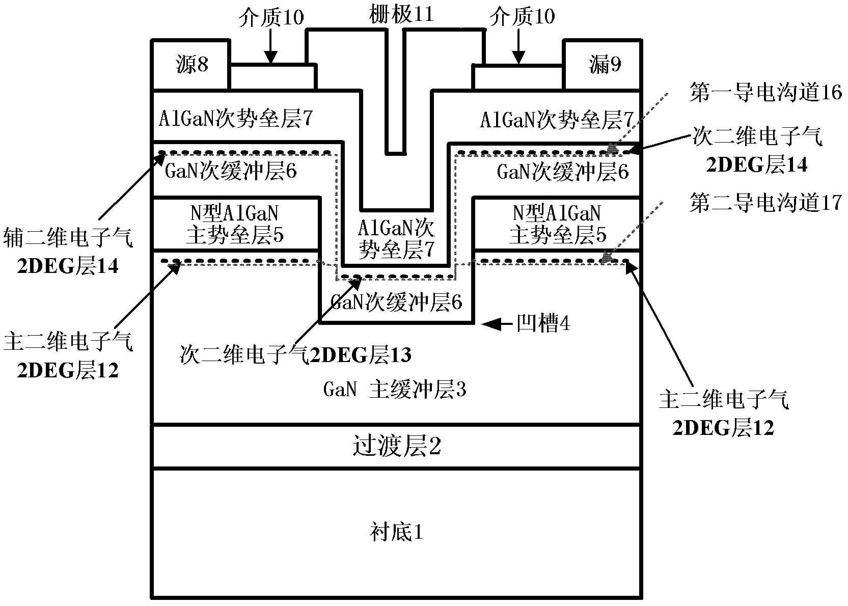
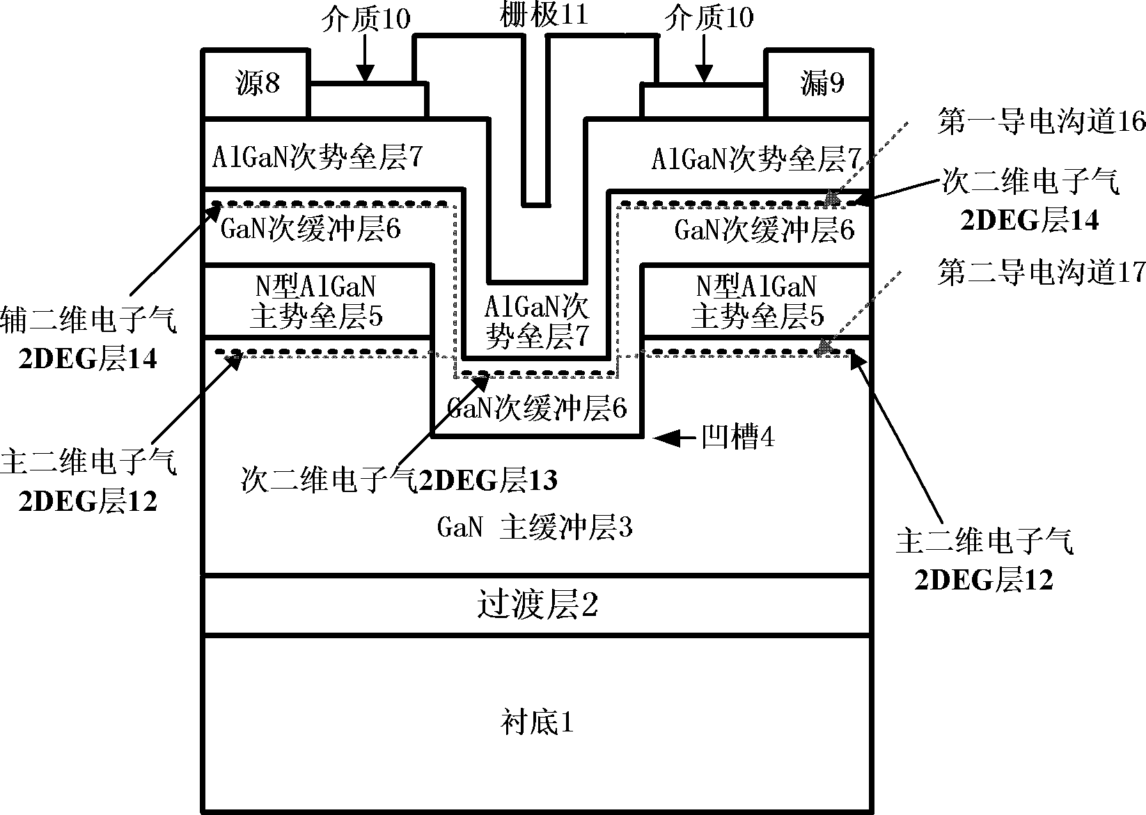
[0049] The thickness of the GaN main buffer layer is 1.2um, Al 0.4 Ga 0.6 The thickness of the N main barrier layer is 15nm, the groove etching depth is 40nm, the thickness of the GaN sub-buffer layer is 24nm, Al 0.4 Ga 0.6 A GaN-based MS gate-enhanced high electron mobility transistor with a thickness of 15nm for the N-time barrier layer and a thickness of 1nm for the gate dielectric layer, the steps are:

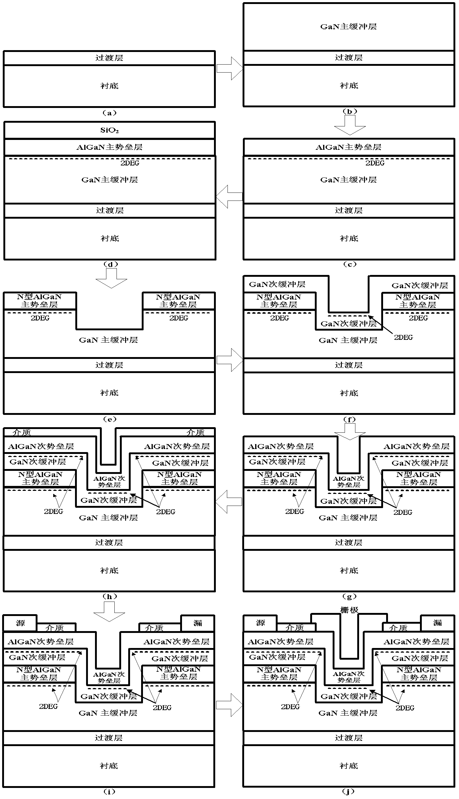
[0050] Step 1, heat treatment and surface nitriding of the substrate:

[0051] Place the sapphire substrate in the metal organic chemical vapor deposition MOCVD reaction chamber, and pump the vacuum degree of the reaction chamber to 1×10 -2Under Torr, under the protection of a mixture of hydrogen with a flow rate of 1500 sccm and ammonia gas with a flow rate of 2000 sccm, heat treatment and surface nitriding of the sapphire substrate are carried out at a heating temperature of 1050° C. and a pressure of 20 Torr.

[0052] Step 2, epitaxial AlN transition layer:

[0053...

Embodiment 2

[0086] The thickness of GaN main buffer layer is 2.5um, Al 0.3 Ga 0.7 The thickness of the N main barrier layer is 28nm, the groove etching depth is 100nm, the thickness of the GaN sub-buffer layer is 70nm, Al 0.3 Ga 0.7 A GaN-based MS gate-enhanced high electron mobility transistor with a thickness of 28nm and a thickness of a gate dielectric layer of 10nm, the steps of which are as follows:

[0087] Step 1 is the same as Step 1 of Embodiment 1.

[0088] Step 2 is the same as Step 2 of Example 1.

[0089] Step 3, using MOCVD technology to epitaxial GaN main buffer layer with a thickness of 2.5um on the AlN transition layer, such as figure 2 (b), the process conditions used for epitaxy are: temperature is 1050° C., pressure is 20 Torr, flow rate of hydrogen gas is 1500 sccm, flow rate of ammonia gas is 6000 sccm, and flow rate of gallium source is 220 sccm.

[0090] Step 4, using MOCVD technology to epitaxially N-type doped Al with a thickness of 28nm on the main buffer ...

Embodiment 3

[0105] The thickness of the GaN main buffer layer is 3.2um, Al 0.18 Ga 0.82 The thickness of the N main barrier layer is 38nm, the groove etching depth is 160nm, the thickness of the GaN sub-buffer layer is 120nm, Al 0.18 Ga 0.82 A GaN-based MS gate-enhanced high electron mobility transistor with a thickness of 38nm and a thickness of a gate dielectric layer of 20nm, the steps of which are as follows:

[0106] Step A is the same as step one of embodiment 1.

[0107] Step B is the same as Step 2 of Example 1.

[0108] Step C, using the process conditions of temperature 1050°C, pressure 20 Torr, hydrogen gas flow rate 1500 sccm, ammonia gas flow rate 6000 sccm, gallium source flow rate 220 sccm, epitaxial GaN main body with a thickness of 3.2um on the AlN transition layer by MOCVD technology buffer layer, such as figure 2 (b).

[0109] Step D, using the process conditions of temperature 920°C, pressure 40Torr, hydrogen flow rate 6000sccm, ammonia flow rate 5000sccm, alumi...


PUM


Abstract

The invention discloses a GaN-based MS grid enhancement type high electron mobility transistor and a manufacture method thereof which mainly resolve the problems of low current density and poor reliability of a GaN-based enhancement type device. The structure of the device is that a transition layer (2) and a GaN main buffer layer (3) are sequentially arranged on a lining (1), a groove (4) is etched in the middle of the GaN main buffer layer, an AlGaN main barrier layer (5) is respectively arranged above the GaN mian buffer layer (3) on two sides of the groove, and a GaN auxiliary buffer layer (6) and an AlGaN auxiliary barrier layer (7) are sequentially arranged on the inner wall of the groove and the surface of the AlGaN main barrier layer (5) on two sides of the groove. A source electrode (8), a drain electrode (9), a grid electrode (11) and a medium layer (10) are arranged on the AlGaN secondary barrier layer (7). The source electrode (8) and the drain electrode (9) are respectively located on two sides above the AlGaN auxiliary barrier layer (7), the grid electrode (11) is located in the middle above the AlGaN auxiliary barrier layer (7), and the medium layer (10) is distributed on an area outside the source electrode, the drain electrode and the grid electrode. The transistor has the advantages of being good in enhancement type characteristic, high in current density, high in breakdown voltage, simple and mature in manufacture process and high in reliability, thereby being capable of being used in high temperature switch devices and digital circuits.

Description

technical field [0001] The invention belongs to the technical field of microelectronics, and relates to semiconductor materials, devices and manufacturing techniques thereof. Specifically, it is a GaN-based MS gate enhanced high electron mobility transistor and its manufacturing method, which can be used in high-temperature and high-power applications and basic units of digital circuits. Background technique [0002] With the development of modern weaponry and aerospace, nuclear energy, communication technology, automotive electronics, and switching power supplies, higher requirements are placed on the performance of semiconductor devices. As a typical representative of wide bandgap semiconductor materials, GaN-based materials have the characteristics of large bandgap width, high electron saturation drift velocity, high critical breakdown field strength, high thermal conductivity, good stability, corrosion resistance, and radiation resistance. Used in the production of high...

Claims


Application Information

Patent Timeline
Patent Type & Authority Applications(China)
IPC IPC(8): H01L29/778H01L29/04H01L29/10H01L21/335
CPCH01L29/66462H01L29/2003H01L29/42316H01L29/7789
Inventor 张进成张琳霞郝跃马晓华王冲艾姗周昊李小刚霍晶张宇桐
Owner 云南凝慧电子科技有限公司
Why Eureka
Try Eureka