Isotropic anthryl compound with oxygen atom substituents, preparation method and application
An isotropic, oxygen atom technology, applied in the field of anthracene-based organic semiconductor materials and their preparation, can solve the problems of poor photostability, cost and stability gap, etc., and achieve low cost, good morphology stability, high charge The effect of transmission performance
- Summary
- Abstract
- Description
- Claims
- Application Information
AI Technical Summary
Problems solved by technology
Method used
Image

Examples
Embodiment 1
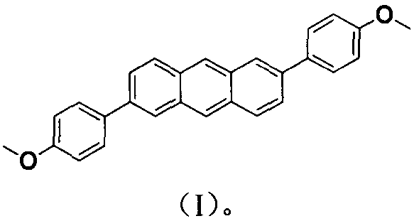
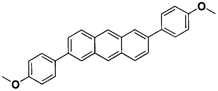
[0019] A heteroatom-substituted anthracene-based organic semiconductor material 2,6-bis(4-methoxybenzene)anthracene (named BOPAnt), its structural formula is:
[0020]
[0021] The method for preparing the organic semiconductor material DOBAnt includes the following steps:
[0022]
[0023] In a 250ml single-mouth reaction flask, add 3.36g 2,6-dibromoanthracene (10mmol), 150ml toluene, 3.80g methoxyphenyl borate (25mmol), 25ml, 2M sodium carbonate solution, 0.23g four (Triphenylphosphine) palladium (0.2 mmol), 2.7 g of trioctyl methyl ammonium chloride, nitrogen gas was passed through the reaction solution for 25 minutes, the reactor was closed, and the temperature was raised to 95° C. and refluxed for 24 hours to terminate the reaction. Wash with methanol, dilute acid solution, acetone and chloroform in sequence, and filter to obtain 2.95 g of yellow product (yield 75.64%), and the obtained product is BOPAnt.
[0024] Check with a thermogravimetric analyzer (TGA). The analysis cond...
Embodiment 2
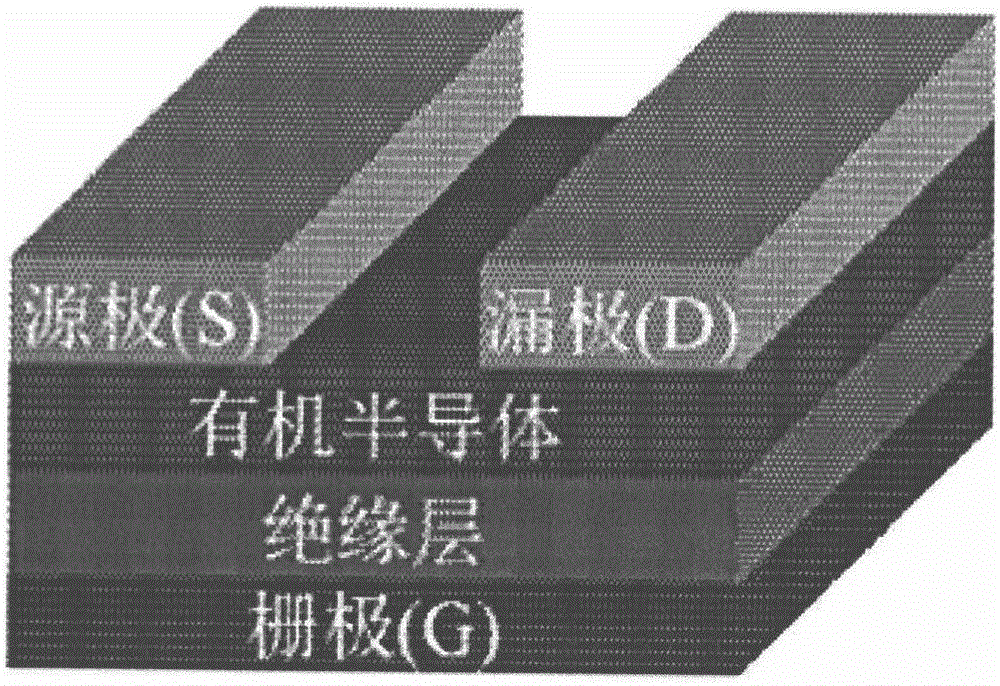
[0028] Preparation of BOPAnt organic field effect transistor
[0029] Step 1: Silicon wafer cleaning
[0030] Prepare a number of 30mm×30mm silicon wafers with an inorganic insulating layer of silicon dioxide on one side, and wash them with deionized water, isopropanol, and acetone in order for 10 minutes, and add a mixed solution of hydrogen peroxide and concentrated sulfuric acid in a ratio of 3:7. Heat at 90°C for 30 minutes, and then clean the silicon wafer with deionized water. Then it was sonicated with isopropanol for 10 minutes and dried with nitrogen.
[0031] Step 2: Device preparation
[0032] The cleaned silicon wafer was taken, and the organic semiconductor material AlDOBAnt prepared in Example 1 was deposited by a vacuum thermal deposition method, the vacuum pressure was 6×10⁻⁴ Pa, the heat flow rate was 0.02, and the thickness of the organic semiconductor was about 50 nm. The drain-source electrode is deposited by a vacuum mask thermal evaporation method with a thickn...
Embodiment 3
[0035] Preparation of BOPAnt organic single crystal field effect transistor.
[0036] Step 1: Silicon wafer cleaning
[0037] Prepare a number of 30mm×30mm silicon wafers with an inorganic insulating layer of silicon dioxide on one side, and wash them with deionized water, isopropanol, and acetone in order for 10 minutes, and add a mixed solution of hydrogen peroxide and concentrated sulfuric acid in a ratio of 3:7 Heat at 90°C for 30 minutes, then clean the silicon wafer with deionized water. Then it was sonicated with isopropanol for 10 minutes and dried with nitrogen. Surface treatment of the substrate and use
[0038] Step 2: Single crystal growth and device preparation on the substrate
[0039] Use vapor phase physical method (PVT) for single crystal growth. Place the cleaned silicon wafer in the crystal growth zone of a multi-temperature tube furnace, place the material in the material sublimation zone, set the temperature in the sublimation zone to 330 degrees Celsius, and cr...
PUM
| Property | Measurement | Unit |
|---|---|---|
| thickness | aaaaa | aaaaa |
Abstract
Description
Claims
Application Information
 - R&D
- Intellectual Property
- Life Sciences
- Materials
- Tech Scout
- Unparalleled Data Quality
- Higher Quality Content
- 60% Fewer Hallucinations
Browse by: Latest US Patents, China's latest patents, Technical Efficacy Thesaurus, Application Domain, Technology Topic, Popular Technical Reports.
© 2025 PatSnap. All rights reserved.Legal|Privacy policy|Modern Slavery Act Transparency Statement|Sitemap|About US| Contact US: help@patsnap.com